📝 2 Sep 2023
In olden days we’d peek and poke the Display Controller, to see weird and wonderful displays.
Today (46 years later), we poke around the Display Controller of Star64 JH7110 RISC-V SBC with a modern tool (not BASIC): U-Boot Bootloader!
(Spoiler: No weird and wonderful displays for today!)
In this article we discover…
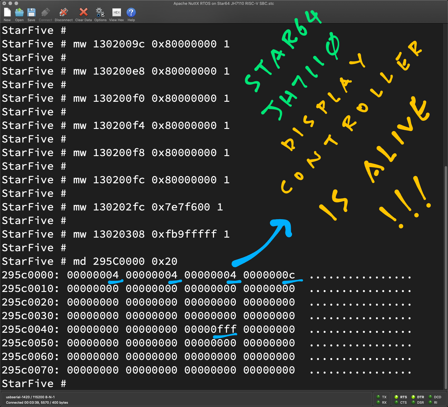
U-Boot Commands md and mw for Dumping and Writing Memory (Pic above)
That we use to power up the Video Output and Display Controller on the StarFive JH7110 SoC
By modding the JH7110 Registers for Power Management Unit, Clock and Reset
Also how we’ll create our own Display Driver for JH7110
In spite of the Missing and Incorrect Docs
Why are we doing this?
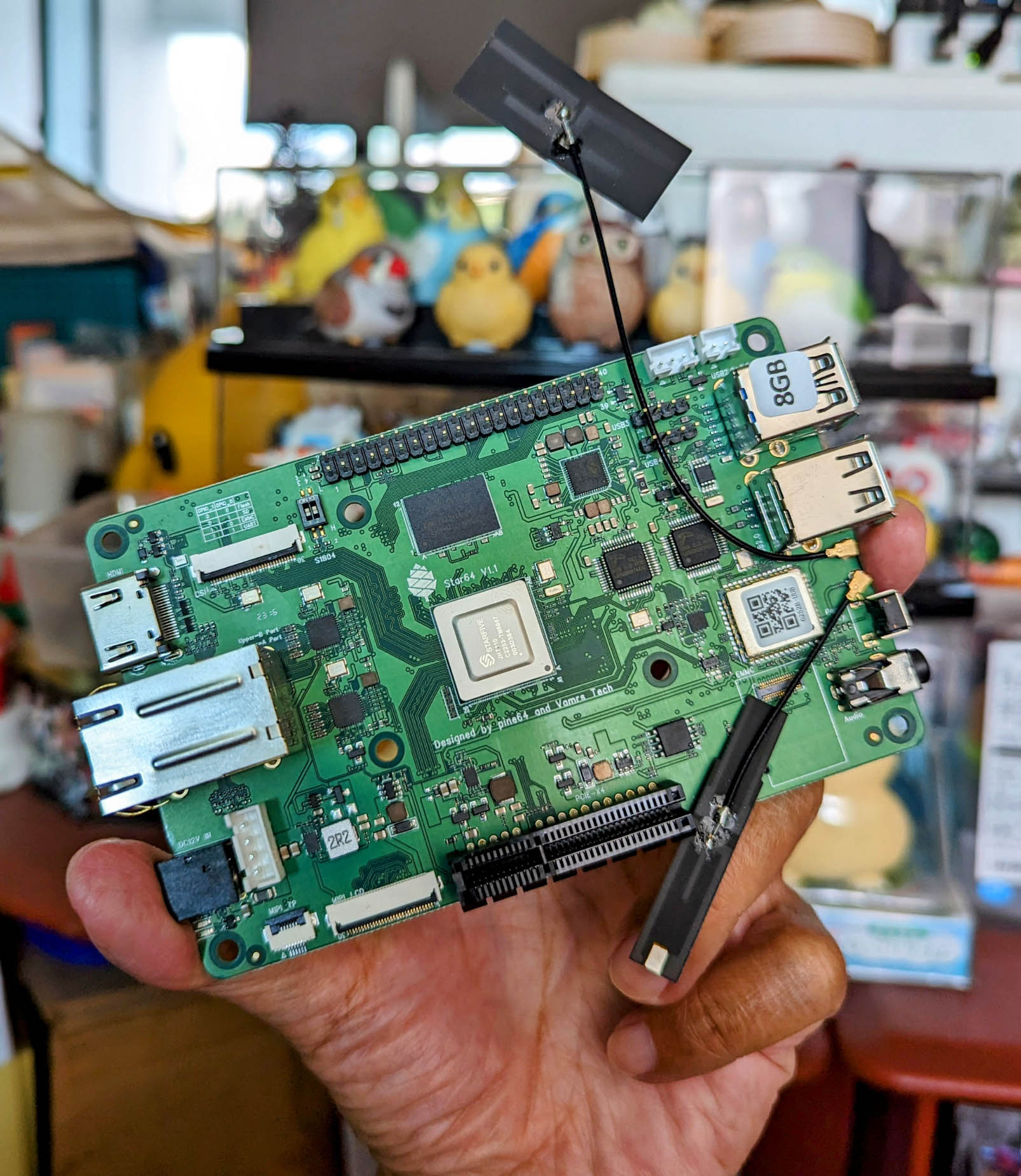
We’re building a HDMI Display Driver for Apache NuttX Real-Time Operating System (RTOS) on the Star64 SBC. (And probably for VisionFive2 too)
The analysis in this article will be super useful for creating our HDMI Driver for NuttX on Star64. (Pic below)
And hopefully this article will be helpful for porting other Operating Systems to JH7110! FreeBSD, Haiku, Multiplix, …
Our Bootloader will Read AND Write any Memory?
Yep! Inside our Star64 SBC is the powerful (maybe risky) U-Boot Bootloader that will read and write JH7110 SoC Memory: RAM, ROM, even I/O Registers!
(ROM is read-only of course)
Boot Star64 without a microSD Card and shut down our TFTP Server. We should see the U-Boot Prompt.
The md command will dump JH7110 Memory (RAM, ROM, I/O Registers)…
# md
md - memory display
Usage: md [.b, .w, .l, .q] address [# of objects]
This is how we dump the JH7110 Boot ROM at 0x2A00 0000…
# md 2A000000 0x20
2a000000: 00000297 12628293 30529073 30005073  ......b.s.R0sP.0
2a000010: 30405073 41014081 42014181 43014281  sP@0.@.A.A.B.B.C
2a000020: 44014381 45014481 46014581 47014681  .C.D.D.E.E.F.F.G
2a000030: 48014781 49014881 4a014981 4b014a81  .G.H.H.I.I.J.J.K
2a000040: 4c014b81 4d014c81 4e014d81 4f014e81  .K.L.L.M.M.N.N.O
2a000050: 01974f81 8193d710 02970ae1 82930000  .O..............
(Cute Alphabet Soup. Where’s the Source, Luke?)
This works for I/O Registers?
Indeed! We can dump the JH7110 UART Registers at 0x1000 0000…
# md 10000000 0x20
10000000: 0000006d 00000000 000000c1 00000003  m...............
10000010: 00000003 00000000 00000000 00000000  ................
10000020: 00000000 00000000 00000000 00000000  ................
10000030: 00000064 00000064 00000064 00000064  d...d...d...d...
What about writing to I/O Registers?
Yep we can write to a UART Register. The mw command writes to JH7110 Memory…
# mw
mw - memory write (fill)
Usage: mw [.b, .w, .l, .q] address value [count]
(Hmmm sounds like a scary Security Risk)
To print something on UART, we poke 0x2A into the UART Transmit Register at 0x1000 0000…
# mw 10000000 2a 1
*
It prints “*”, equivalent to ASCII Code 0x2A!
Moving to something more sophisticated: JH7110 Display Controller…
Dumping the JH7110 Display Controller should work right?
We’ll find out! Based on…
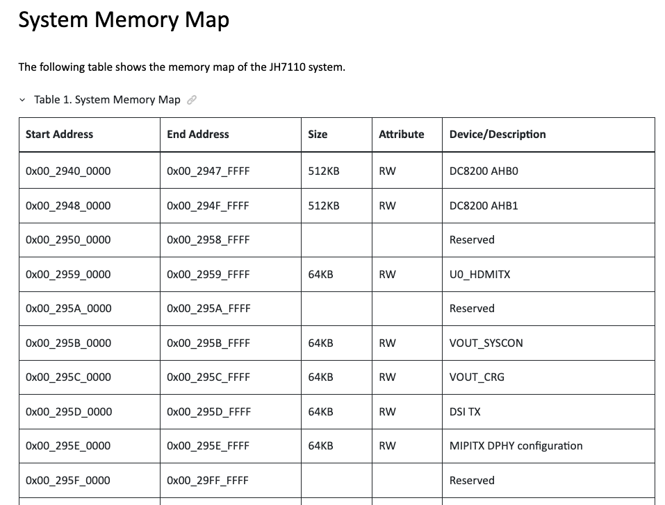
The registers for JH7110 Display Subsystem (pic above) are at…
| Address | Display Registers |
|---|---|
0x2940 0000 | DC8200 AHB0 (Display Bus 0) |
0x2948 0000 | DC8200 AHB1 (Display Bus 1) |
0x2959 0000 | U0_HDMITX (HDMI) |
0x295B 0000 | VOUT_SYSCON (System Config) |
0x295C 0000 | VOUT_CRG (Clock and Reset) |
0x295D 0000 | DSI TX (MIPI Display Serial Interface) |
0x295E 0000 | MIPITX DPHY (MIPI Display Physical Layer) |
(DC8200 is the VeriSilicon Dual Display Controller)
We dump the above Display Subsystem Registers…
# md 29400000 0x20
29400000: 00000000 00000000 00000000 00000000  ................
29400010: 00000000 00000000 00000000 00000000  ................

# md 29480000 0x20
29480000: 00000000 00000000 00000000 00000000  ................
29480010: 00000000 00000000 00000000 00000000  ................

# md 29590000 0x20
29590000: 00000000 00000000 00000000 00000000  ................
29590010: 00000000 00000000 00000000 00000000  ................

# md 295B0000 0x20
295b0000: 00000000 00000000 00000000 00000000  ................
295b0010: 00000000 00000000 00000000 00000000  ................

# md 295C0000 0x20
295c0000: 00000000 00000000 00000000 00000000  ................
295c0010: 00000000 00000000 00000000 00000000  ................
But the values are all zero!
That’s because the Display Subsystem is not powered up.
To fix this, we tweak some registers and power up the Display Subsystem…
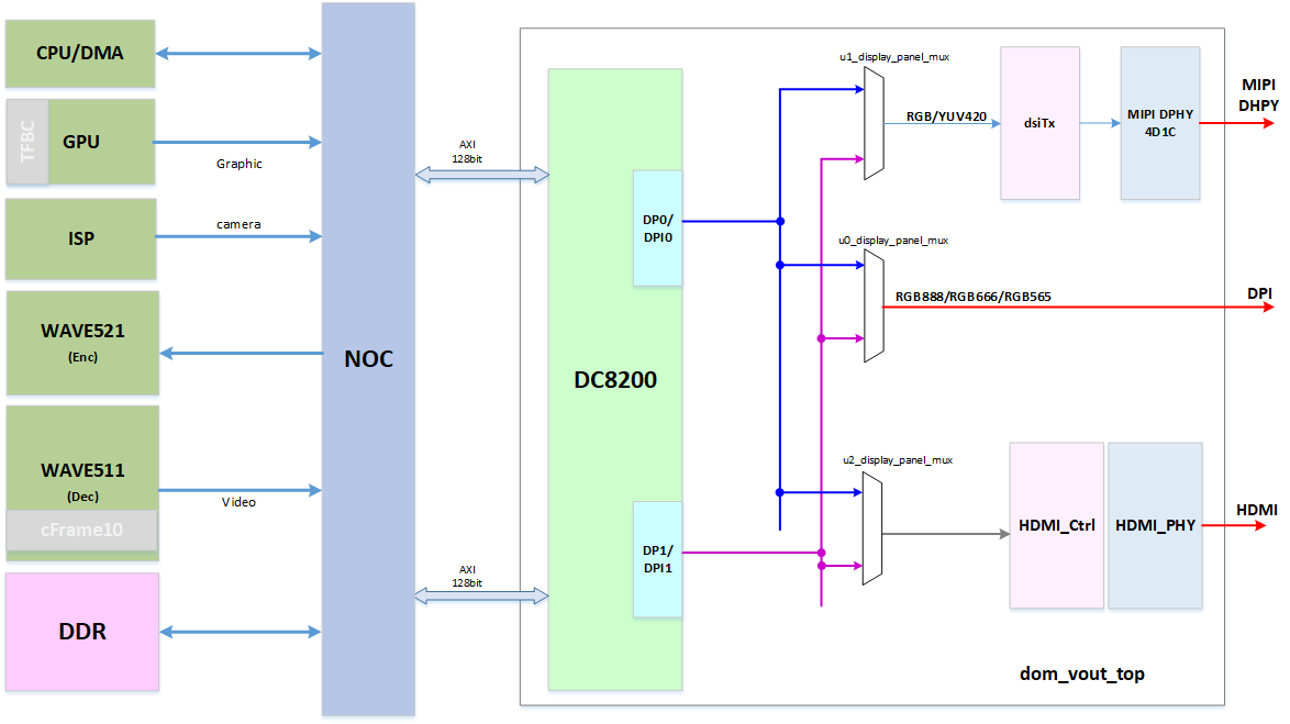
JH7110 Display Subsystem Block Diagram
How to power up the Display Subsystem?
From the pic above, the Display Subsystem is powered in the Video Output Power Domain (DOM_VOUT).
Which is powered by the JH7110 Power Management Unit (PMU)…
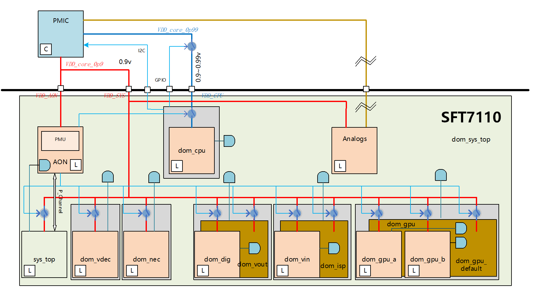
(Not to be confused with External PMIC: X-Powers AXP15060)
Are the lights on for Video Output DOM_VOUT?
To find out, we dump the status of the Power Domains…
From System Memory Map: Base Address of PMU is 0x1703 0000
From PMU Registers: Current Power Mode is at Offset 0x80
Hence the Current Power Mode is at 0x1703 0080. When we dump the register…
# md 17030080 1
17030080: 00000003
Current Power Mode is 3, saying that…
How to power up VOUT?
We read the PMU Function Description…
SW Encourage Turn-on Sequence
(1) Configure the register SW Turn-On Power Mode (Offset
0x0C), write the bit 1 which Power Domain will be turn-on, write the others 0;
(2) Write the SW Turn-On Command Sequence. Write the register Software Encourage (Offset
0x44)0xFF→0x05→0x50
What’s a “Software Encourage”?
Something got Lost in Translation. We assume it means “Software Triggered”.
Thus we set the Power Mode (Offset 0x0C) to 0x10 (Bit 4 for VOUT)…
# mw 1703000c 0x10 1Then we write the Command Sequence at Offset 0x44 (no delays needed)…
# mw 17030044 0xff 1
# mw 17030044 0x05 1
# mw 17030044 0x50 1
Finally we dump the Current Power Mode…
# md 17030080 1
17030080: 00000013
Lights on folks, Video Output Power VOUT (Bit 4) is On!
(Actually we should wait 50 milliseconds to Power Up)
We’re ready to dump the Display Subsystem?
Sadly nope, the Display Subsystem Registers are still empty…
# md 295C0000 0x20
295c0000: 00000000 00000000 00000000 00000000  ................
295c0010: 00000000 00000000 00000000 00000000  ................
We need more mods, for the Clock and Reset Signals…
Display Subsystem (VOUT) is already powered up via the Power Management Unit (PMU)…
Anything else we need to make it work?
Always remember to enable the VOUT Clocks and deassert the VOUT Resets!
According to the JH7110 Clock Structure (pic above), the Display Subsystem (VOUT) is Clocked by…
Plus one Reset…
How to enable the Clocks and deassert the Resets?
We set the System Control Registers (SYS CRG) at Base Address 0x1302 0000
When we match the above Clocks to the System Control Registers (SYS CRG), we get…
| SYS CRG Offset | Clock |
|---|---|
0x28 | Clock AHB 1 |
0x4C | MCLK Out |
0x98 | clk_u0_sft7110_noc_bus _clk_cpu_axi |
0x9C | clk_u0_sft7110_noc_bus _clk_axicfg0_axi |
0xE8 | clk_u0_dom_vout_top _clk_dom_vout_top_clk_vout_src |
0xF0 | Clock NOC Display AXI |
0xF4 | Clock Video Output AHB |
0xF8 | Clock Video Output AXI |
0xFC | Clock Video Output HDMI TX0 MCLK |
(Looks excessive, but better to enable too many Clocks than too few!)
(AXI is the Advanced eXtensible Interface)
To enable the Clocks above, we set Bit 31 (clk_icg) to 1.
Here are the U-Boot Commands to enable the VOUT Clocks…
## Enable the Clocks for Video Output (Display Subsystem)
mw 13020028 0x80000000 1
mw 1302004c 0x80000000 1
mw 13020098 0x80000000 1
mw 1302009c 0x80000000 1
mw 130200e8 0x80000000 1
mw 130200f0 0x80000000 1
mw 130200f4 0x80000000 1
mw 130200f8 0x80000000 1
mw 130200fc 0x80000000 1
What about the Resets?
Digging through the System Control Registers (SYS CRG), we need to deassert these Resets…
Software RESET 1 Address Selector (SYS CRG Offset 0x2FC)
Bit 11: rstn_u0_dom_vout_top _rstn_dom_vout_top_rstn_vout_src
SYSCRG RESET Status 0 (SYS CRG Offset 0x308)
Bit 26: rstn_u0_sft7110_noc_bus _reset_disp_axi_n
SYSCRG RESET Status 1 (SYS CRG Offset 0x30C)
Bit 11: rstn_u0_dom_vout_top _rstn_dom_vout_top_rstn_vout_src
We set the above bits to 0 to deassert the Resets.
First we dump the above VOUT Reset Registers…
# md 130202fc 1
130202fc: 07e7fe00

# md 13020308 1
13020308: ff9fffff

# md 1302030c 1
1302030c: f80001ff
Then we flip the VOUT Reset Bits to 0…
# mw 130202fc 0x07e7f600 1
# mw 13020308 0xfb9fffff 1
(The last Reset is already deasserted, no need to flip it)
What happens when we enable the Clocks and deassert the Resets?
We run the above commands to set the Clocks and Resets.
And again we dump the Display Subsystem (VOUT) Registers…
# md 295C0000 0x20
295c0000: 00000004 00000004 00000004 0000000c  ................
295c0010: 00000000 00000000 00000000 00000000  ................
295c0020: 00000000 00000000 00000000 00000000  ................
295c0030: 00000000 00000000 00000000 00000000  ................
295c0040: 00000000 00000000 00000fff 00000000  ................
The Display Subsystem Registers are finally visible at VOUT CRG 0x295C 0000
Which means the Display Subsystem is alive yay!
(0x295C 000C defaults to 0x0C, there’s a typo in the doc)
Phew that’s a long list of U-Boot Commands. Can we automate this?
## Power Up the PMU for Video Output (Display Subsystem)
mw 1703000c 0x10 1
mw 17030044 0xff 1
mw 17030044 0x05 1
mw 17030044 0x50 1

## Enable the Clocks for Video Output (Display Subsystem)
mw 13020028 0x80000000 1
mw 1302004c 0x80000000 1
mw 13020098 0x80000000 1
mw 1302009c 0x80000000 1
mw 130200e8 0x80000000 1
mw 130200f0 0x80000000 1
mw 130200f4 0x80000000 1
mw 130200f8 0x80000000 1
mw 130200fc 0x80000000 1

## Deassert the Resets for Video Output (Display Subsystem)
mw 130202fc 0x07e7f600 1
mw 13020308 0xfb9fffff 1
md 295C0000 0x20
Sure can!
Run this to create a U-Boot Script that powers up the Display Subsystem…
## Create the U-Boot Script to power up the Video Output
setenv video_on 'mw 1703000c 0x10 1 ; mw 17030044 0xff 1 ; mw 17030044 0x05 1 ; mw 17030044 0x50 1 ; mw 13020028 0x80000000 1 ; mw 1302004c 0x80000000 1 ; mw 13020098 0x80000000 1 ; mw 1302009c 0x80000000 1 ; mw 130200e8 0x80000000 1 ; mw 130200f0 0x80000000 1 ; mw 130200f4 0x80000000 1 ; mw 130200f8 0x80000000 1 ; mw 130200fc 0x80000000 1 ; mw 130202fc 0x07e7f600 1 ; mw 13020308 0xfb9fffff 1 ; md 295C0000 0x20 ; '

## Check that it's correct
printenv video_on

## Save it for future reboots
saveenv

## Run the U-Boot Script to power up the Video Output
run video_on
The U-Boot Script video_on is saved into our SBC’s Internal Flash Memory.
Which means we can switch on our SBC and run the script anytime…
# run video_on
295c0000: 00000004 00000004 00000004 0000000c  ................
295c0010: 00000000 00000000 00000000 00000000  ................
295c0020: 00000000 00000000 00000000 00000000  ................
295c0030: 00000000 00000000 00000000 00000000  ................
295c0040: 00000000 00000000 00000fff 00000000  ................
So much easier to power up the Display Subsystem!
Next we do the Display Controller…
JH7110 Display Subsystem Clock and Reset
JH7110 Display Subsystem is already powered up…
What about the Display Controller?
Nope our DC8200 Display Controller (DC8200 AHB0) is stil invisible…
# md 29400000 0x20
29400000: 00000000 00000000 00000000 00000000  ................
29400010: 00000000 00000000 00000000 00000000  ................
What about the Clocks and Resets for the Display Controller?
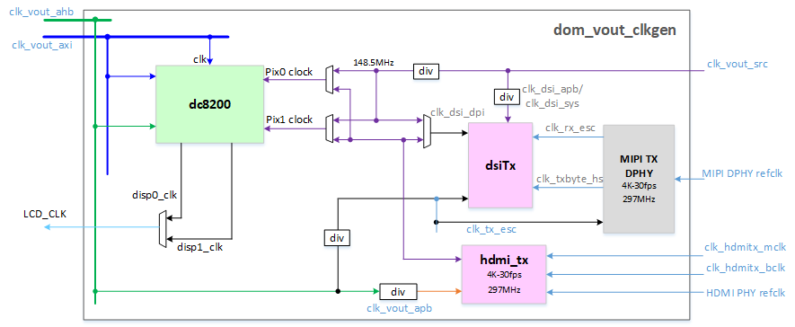
The pic above shows the Display Controller Clocks and Resets.
According to the VOUT CRG (Video Output Clock and Reset Registers), these are the DC8200 Clock Registers for HDMI…
| VOUT CRG Offset | Clock |
|---|---|
0x10 | clk_u0_dc8200_clk_axi |
0x14 | clk_u0_dc8200_clk_core |
0x18 | clk_u0_dc8200_clk_ahb |
0x1C | clk_u0_dc8200_clk_pix0 |
0x20 | clk_u0_dc8200_clk_pix1 |
0x3C | clk_u0_hdmi_tx_clk_mclk |
0x40 | clk_u0_hdmi_tx_clk_bclk |
0x44 | clk_u0_hdmi_tx_clk_sys |
To enable the Clocks above, we set Bit 31 (clk_icg) to 1.
(VOUT CRG Base Address is 0x295C 0000)
DC8200 Resets for HDMI are at Software_RESET_assert0_addr_assert_sel (VOUT CRG Offset 0x48)…
Bit 0: rstn_u0_dc8200_rstn_axi
Bit 1: rstn_u0_dc8200_rstn_ahb
Bit 2: rstn_u0_dc8200_rstn_core
Bit 9: rstn_u0_hdmi_tx_rstn_hdmi
We set the above bits to 0 to deassert the Resets.
(DC8200 Reset Register is mislocated in the docs)
These are the U-Boot Commands to set the DC8200 Clocks and Resets for HDMI…
## Power up the Video Output (Display Subsystem)
run video_on

## Enable the DC8200 HDMI Clocks
mw 295C0010 0x80000000 1
mw 295C0014 0x80000000 1
mw 295C0018 0x80000000 1
mw 295C001c 0x80000000 1
mw 295C0020 0x80000000 1
mw 295C003c 0x80000000 1
mw 295C0040 0x80000000 1
mw 295C0044 0x80000000 1

## Deassert the DC8200 HDMI Resets.
## We deassert all Resets for today.
mw 295C0048 0 1
Does it work?
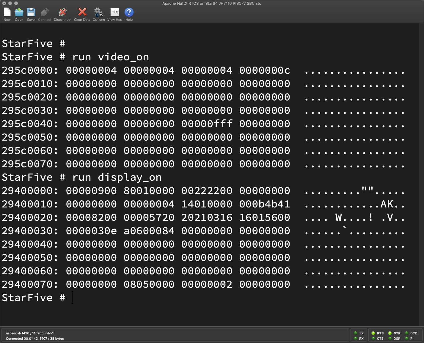
We run the above U-Boot Commands for VOUT HDMI. Then we dump our DC8200 Display Controller (DC8200 AHB0)…
# md 29400000 0x20
29400000: 00000900 80010000 00222200 00000000  ........."".....
29400010: 00000000 00000004 14010000 000b4b41  ............AK..
29400020: 00008200 00005720 20210316 16015600  .... W....! .V..
29400030: 0000030e a0600084 00000000 00000000  ......`.........
Yep our DC8200 Display Controller is finally alive yay!
Based on the above commands, we write the U-Boot Script to start the Display Controller (pic below)…
## Create the U-Boot Script to power up the Display Controller
setenv display_on 'mw 295C0010 0x80000000 1 ; mw 295C0014 0x80000000 1 ; mw 295C0018 0x80000000 1 ; mw 295C001c 0x80000000 1 ; mw 295C0020 0x80000000 1 ; mw 295C003c 0x80000000 1 ; mw 295C0040 0x80000000 1 ; mw 295C0044 0x80000000 1 ; mw 295C0048 0 1 ; md 29400000 0x20 ; '

## Check that it's correct
printenv display_on

## Save it for future reboots
saveenv

## Run the U-Boot Script to power up the Video Output
run video_on

## Run the U-Boot Script to power up the Display Controller
run display_onOne last thing: We verify the DC8200 Register Values…
Are the DC8200 Register Values correct?
According to the DC8200 Display Driver, we can sniff these Register Values from the DC8200 Display Controller…
Hardware Revision: DC8200 AHB0 Offset 0x24
Chip ID: DC8200 AHB0 Offset 0x30
This is how we dump the Hardware Revision and Chip ID in U-Boot…
## Power up the Video Output
run video_on

## Power up the Display Controller
run display_on

## TODO: Wait 500 milliseconds to Power Up

## Dump the Hardware Revision
md 29400024 1

## Dump the Chip ID
md 29400030 1
We should see…
# md 29400024 1
29400024: 00005720

# md 29400030 1
29400030: 0000030e
That means…
Hardware Revision is 0x5720 (DC_REV_0)
Chip ID is 0x30E
Our DC8200 Display Controller returns the correct Register Values yay!
(Do we have a Date at 0x2940 0028? It reads “20210316”)
How will we create the NuttX Display Driver for JH7110?
Earlier we talked about the steps to power up the Display Subsystem and Display Controller…
This is how we implement the steps in our NuttX Display Driver: jh7110_appinit.c
// Power Up the Power Management Unit
// for Video Output / Display Subsystem
// TODO: Switch to constants
putreg32(0x10, 0x1703000c);
putreg32(0xff, 0x17030044);
putreg32(0x05, 0x17030044);
putreg32(0x50, 0x17030044);
This code will power up the Display Subsystem via the Power Management Unit.
(Yeah needs cleanup)
Next we enable the VOUT Clocks and deassert the VOUT Resets for the Display Subsystem…
// Enable the Clocks for Video Output / Display Subsystem
modifyreg32(0x13020028, 0, 1 << 31);  // Addr, Clear Bits, Set Bits
modifyreg32(0x1302004c, 0, 1 << 31);
modifyreg32(0x13020098, 0, 1 << 31);
modifyreg32(0x1302009c, 0, 1 << 31);
modifyreg32(0x130200e8, 0, 1 << 31);
modifyreg32(0x130200f0, 0, 1 << 31);
modifyreg32(0x130200f4, 0, 1 << 31);
modifyreg32(0x130200f8, 0, 1 << 31);
modifyreg32(0x130200fc, 0, 1 << 31);

// Deassert the Resets for Video Output / Display Subsystem
modifyreg32(0x130202fc, 1 << 11, 0);  // Addr, Clear Bits, Set Bits
modifyreg32(0x13020308, 1 << 26, 0);

// Verify that Video Output / Display Subsystem is up
val = getreg32(0x295C0000);
DEBUGASSERT(val == 4);
Then we do the same for the Display Controller…
// Enable the Clocks for DC8200 Display Controller (HDMI)
modifyreg32(0x295C0010, 0, 1 << 31);  // Addr, Clear Bits, Set Bits
modifyreg32(0x295C0014, 0, 1 << 31);
modifyreg32(0x295C0018, 0, 1 << 31);
modifyreg32(0x295C001c, 0, 1 << 31);
modifyreg32(0x295C0020, 0, 1 << 31);
modifyreg32(0x295C003c, 0, 1 << 31);
modifyreg32(0x295C0040, 0, 1 << 31);
modifyreg32(0x295C0044, 0, 1 << 31);

// Deassert the Resets for DC8200 Display Controller (HDMI)
modifyreg32(
  0x295C0048,  // Addr
  (1 << 0) | (1 << 1) | (1 << 2) | (1 << 9),  // Clear Bits
  0  // Set Bits
);
Finally we check the Hardware Revision and Chip ID…
// TODO: Power up ALDO3 and ALDO5 on the External Power Management IC
// (X-Powers AXP15060 PMIC over I2C)
// (I2C SCL on GPIO 19, SDA on GPIO 20)

// Wait 500 milliseconds to Power Up PMIC
up_mdelay(500);

// Verify that Hardware Revision and Chip ID are non-zero
uint32_t revision = getreg32(0x29400024);
uint32_t chip_id  = getreg32(0x29400030);
_info("revision=0x%x, chip_id=0x%x", revision, chip_id);
DEBUGASSERT(revision != 0 && chip_id != 0);
Does it work with NuttX?
Yep NuttX will start our Display Driver and print the Hardware Revision and Chip ID…
Starting kernel...
board_late_initialize:
  revision=0x5720
  chip_id=0x30e
  hdmi_status=0x30

NuttShell (NSH) NuttX-12.0.3
nsh>
But our HDMI Status says that Hot Plug is Disconnected.
(Probably because our ALDOs are missing)
What about the rest of the Display Driver?
The remaining steps are described here…
But we have a problem with Incomplete and Incorrect Docs, see the next section.
Who starts our Display Driver?
At Startup, our NuttX Driver will be called from board_late_initialize.
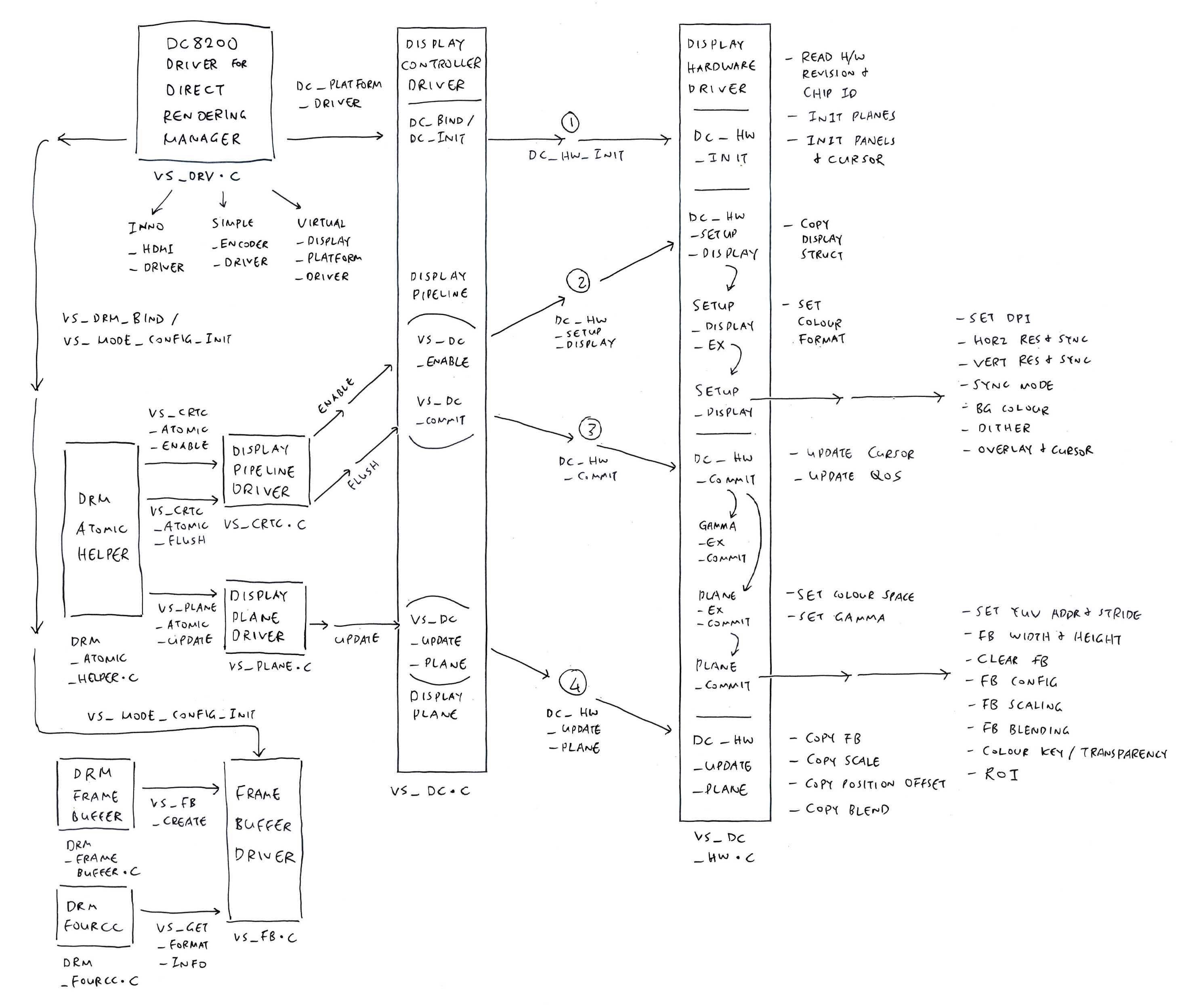
Official Display Driver for JH7110
Are we done with our NuttX Display Driver?
Not quite! We have a couple of challenges with Incomplete and Incorrect Docs…
What are these Mystery Writes to Undocumented Registers in the DC8200 Display Controller?
Reset Register for Video Output (VOUT) seems to be misplaced…
How to set the VOUT Clock Source?
How to set the VOUT Clock Rate?
Typo in the VOUT Clock Default Rate…
Indeed Software is Encouraging, but we’ll make our own interpretation…
Hopefully we’ll overcome these issues and complete our NuttX Display Driver!
Today we did some cool things with U-Boot Bootloader on JH7110 SoC…
We ran the U-Boot Commands md and mw for reading and writing JH7110 Memory
We powered up the Video Output and Display Controller on the JH7110 SoC
By modding the JH7110 Registers for Power Management Unit, Clock and Reset
We’re one step closer to creating our NuttX Display Driver for JH7110
Hopefully we’ll see many other Display Drivers for JH7110: FreeBSD, Haiku, Multiplix, …
Now we need an I2C Driver for JH7110, to power up the External Power Management IC. Which we’ll cover in the next article!
Many Thanks to my GitHub Sponsors (and the awesome NuttX Community) for supporting my work! This article wouldn’t have been possible without your support.
Got a question, comment or suggestion? Create an Issue or submit a Pull Request here…
lupyuen.github.io/src/display3.md
Based on everything we deciphered in this article and the previous one…
The JH7110 Display Driver (HDMI) that we create for NuttX (and other Operating Systems) shall do the following…
Power Up the Power Management Unit for Video Output (Display Subsystem)
Wait 50 milliseconds to Power Up
Enable the Clocks for Video Output (Display Subsystem)
Deassert the Resets for Video Output (Display Subsystem)
Verify that Video Output (Display Subsystem) is up
Enable the Clocks for DC8200 Display Controller (HDMI)
Deassert the Resets for DC8200 Display Controller (HDMI)
Power up ALDO3 (1.8V) and ALDO5 (0.9V) on the External Power Management IC
Wait 500 milliseconds to Power Up PMIC
Verify that Hardware Revision and Chip ID are non-zero
Read the HDMI Status, check for Hot Plug
Detect HDMI
Disable HDMI Transmit PHY
Configure HDMI Transmit PHY for 1080p 60 Hz
Enable HDMI Transmit PHY
Enable HDMI TMDS
Enable HDMI Data Sync
Set the Clock Source of u0_dc8200.clk_pix0 to clk_dc8200_pix0
Set the Clock Rate of dc8200_pix0 to 148.5 MHz (HDMI Clock)
Bunch of Mystery Writes to DC8200 AHB0
TODO: How to write to Framebuffer?
Shall we check the Official Linux Driver? (Pic below)
Why is the HDMI Display Unstable?
Our JH7110 Display Driver is partially implemented here: jh7110_appinit.c
TODO: Implement the JH7110 I2C Driver (based on DesignWare I2C) so we can control the PMIC. This NuttX I2C Driver might work: cxd56_i2c.c
(Many Thanks to Justin / Fishwaldo for recommending the HDMI Driver from U-Boot Bootloader)
Official Display Driver for JH7110
In this section we talk about the Missing, Mistaken and Mysterious things in the JH7110 Display Controller.
We spoke about our JH7110 Display Driver and a Bunch of Mystery Writes…
Inside the U-Boot Display Driver (officially contributed by StarFive), there’s a long list of Mystery Writes to Undocumented Registers in the DC8200 Display Controller: sf_vop.c
writel(0xc0001fff, priv->regs_hi+0x00000014);
writel(0x00002000, priv->regs_hi+0x00001cc0);
//writel(uc_plat->base+0x1fa400, priv->regs_hi+0x00001530);
writel(0x00000000, priv->regs_hi+0x00001800);
writel(0x00000000, priv->regs_hi+0x000024d8);
writel(0x021c0780, priv->regs_hi+0x000024e0);
writel(0x021c0780, priv->regs_hi+0x00001810);
...(regs_hi is DC8200 AHB0 Base Address 0x2940 0000)
Plus this super baffling one…
writel(uc_plat->base, priv->regs_hi+0x00001400);What’s happening here?
Shall we match the Mystery Writes with the Official Linux Driver? (Pic above)

Software_RESET_assert0_addr_assert_sel
DC8200 Reset Register Software_RESET_assert0_addr_assert_sel is actually at Offset 0x48, Address 0x295C 0048.
(Instead of Offset 0x38, pic above)
How did we figure out it’s at Offset 0x48?
Clearing the Reset Bits at Offset 0x38 (and Offset 0x4C) has no effect, according to our testing.
Thanks to U-Boot, we have this dump of the VOUT Clock and Reset Registers (CRG)…
# md 295C0000 0x20
295c0000: 00000004 00000004 00000004 0000000c  ................
295c0010: 00000000 00000000 00000000 00000000  ................
295c0020: 00000000 00000000 00000000 00000000  ................
295c0030: 00000000 00000000 00000000 00000000  ................
295c0040: 00000000 00000000 00000fff 00000000  ................
Offset 0x38 is 0, which doesn’t look right for a Reset Register that should be filled with “1” Bits (by default).
Then we noticed that Offset 0x48 is filled with “1” Bits: 0xFFF. Thus we cleared the Reset Bits at Offset 0x48, and it works!

How to set the Clock Source of u0_dc8200.clk_pix0 to clk_dc8200_pix0?
clk_u0_dc8200_clk_pix0 is at Offset 0x1C (Pic above)
Bits 24 to 29: clk_mux_sel (Default 0)
Clock multiplexing selector:
But what are the valid values for clk_mux_sel?
Can we read another Multiplexed Clock to figure out the valid values?
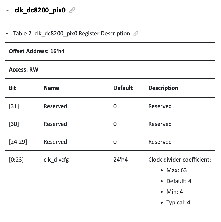
How to set the Clock Rate of dc8200_pix0 to 148.5 MHz? (HDMI Clock)
clk_dc8200_pix0 is at Offset 0x04 (Pic above)
Bits 0 to 23: clk_divcfg (Default 4)
Clock divider coefficient:
Max: 63 (307.2 MHz?), Default: 4, Min: 4, Typical: 4
What is the Clock Divider value we should set?
What is the Input Frequency to the Clock? 307.2 MHz?
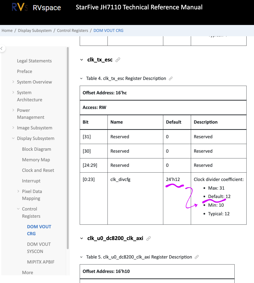
clk_tx_esc at Offset 0x0C (Address 0x295C 000C) should have default 24'hc. (Equivalent to 0x0C)
There’s a typo in the doc, it shows default 24'h12 (Pic above)
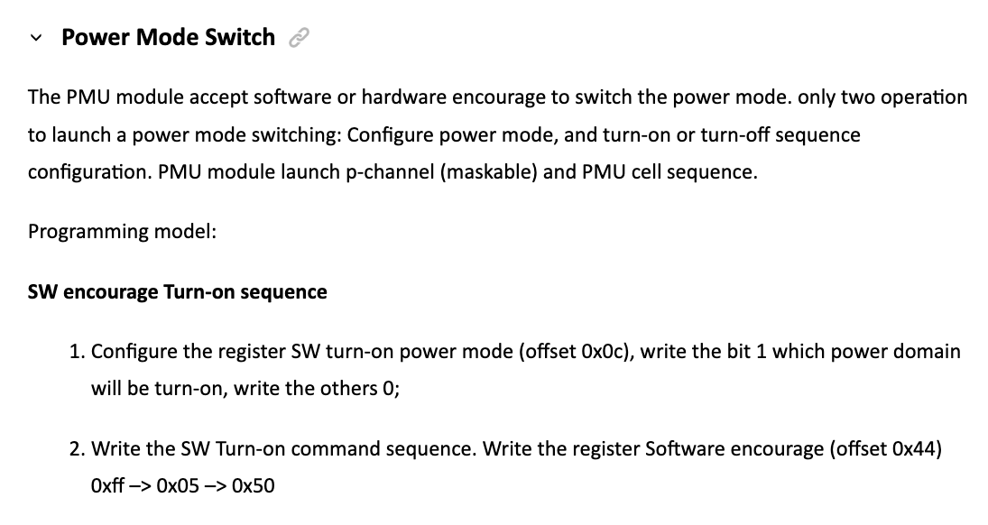
From the Power Management Unit (PMU) Function Description (pic above)…
SW Encourage Turn-on Sequence
(1) Configure the register SW Turn-On Power Mode (Offset
0x0C), write the bit 1 which Power Domain will be turn-on, write the others 0;
(2) Write the SW Turn-On Command Sequence. Write the register Software Encourage (Offset
0x44)0xFF→0x05→0x50
What’s a “Software Encourage”?
Something got Lost in Translation. We assume it means “Software Triggered”.