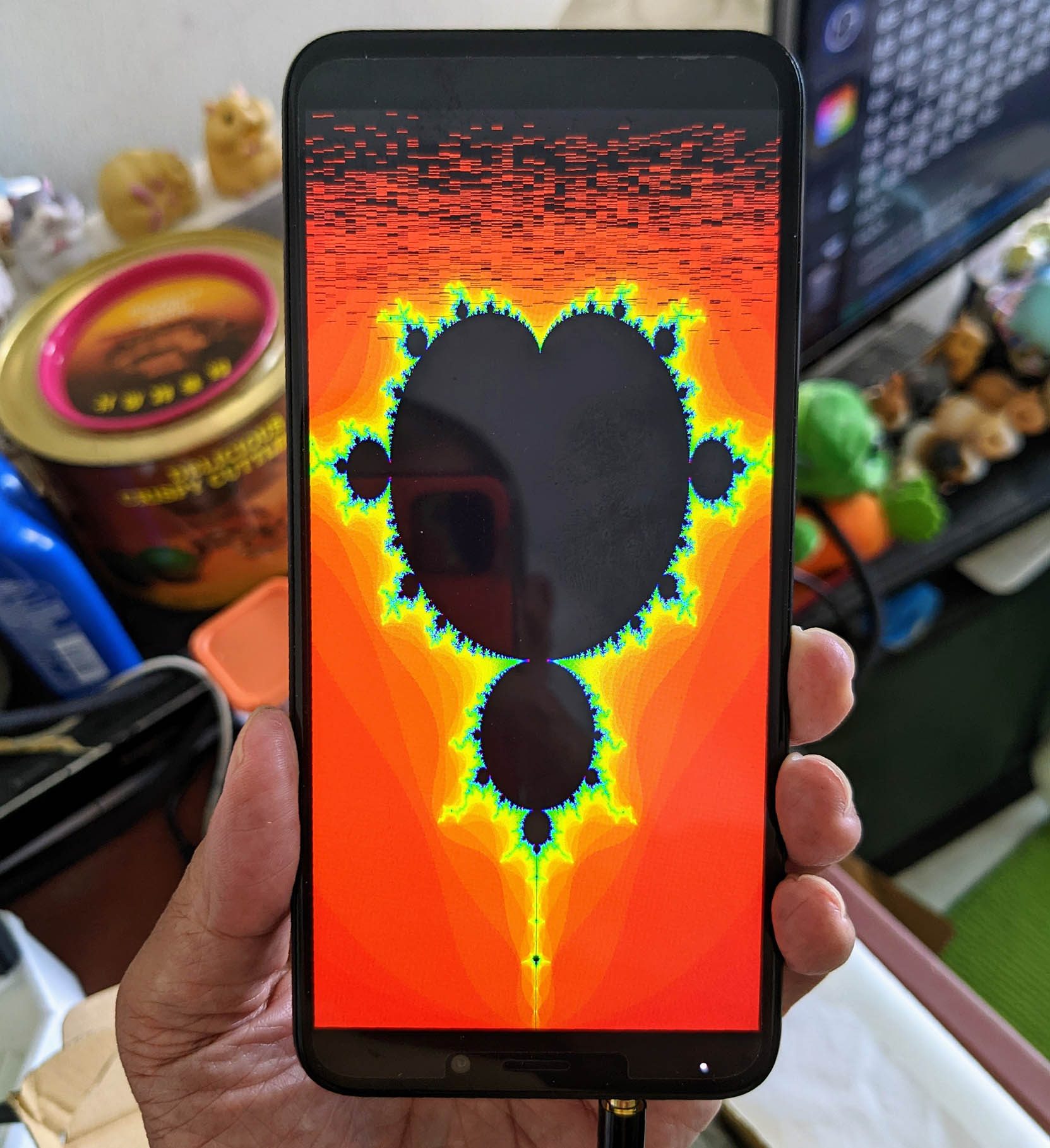
📝 30 Oct 2022

PinePhone rendering Mandelbrot Set on Apache NuttX RTOS
UPDATE: PinePhone is now officially supported by Apache NuttX RTOS (See this)
In the last 2 articles we talked about Pine64 PinePhone (pic above) and how we built a Display Driver for PinePhone’s MIPI Display Serial Interface…
But our PinePhone Display Driver isn’t complete… It won’t render any graphics!
Today we’ll learn about the missing bits in our Display Driver…
What’s the Display Engine (DE) inside PinePhone
How the Timing Controller (TCON0) controls PinePhone’s LCD Display
How we call DE and TCON0 to render graphics
How our new PinePhone Display Driver will support DE and TCON0
Why are we doing this?
We’re now porting Apache NuttX RTOS to PinePhone and we have created a (barebones) Display Driver in Zig that initialises the LCD Display.
To finish the driver, we need to understand what’s inside PinePhone’s Display Engine and Timing Controller.
Let’s dive in and continue the journey from our (super long) NuttX Porting Journal…
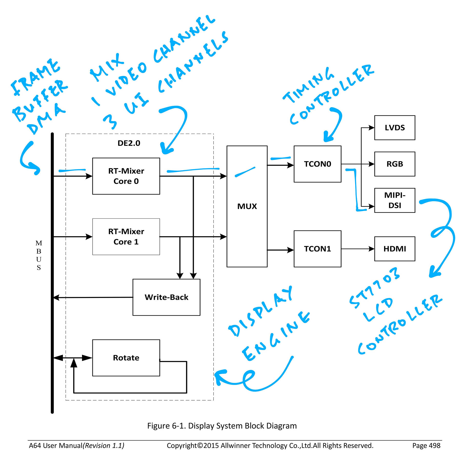
Display Engine (DE) and Timing Controller (TCON0) from A64 User Manual (Page 498)
Suppose we’re building our own Operating System for PinePhone…
How do we render graphics on the LCD Display?
Rendering graphics directly to PinePhone Hardware (“Bare Metal”) is more complicated than we expect!
Let’s walk through the steps (pic above)…
Inside PinePhone’s Allwinner A64 SoC is a Display Engine that combines and transforms Pixel Data for display
The Display Engine reads the Pixel Data from Framebuffers in RAM via Direct Memory Access (DMA)
(Up to 3 Framebuffers)
Inside the Display Engine is a Real-Time Mixer (RT Mixer Core 0) that handles real-time DMA, Overlay, Scaling and Blending of the Pixel Data (from the Framebuffers)
(We won’t need RT Mixer Core 1 today, it’s a smaller version of Core 0)
The Real-Time Mixer supports 3 UI Channels (for graphics), all mixed together into a Single Image Frame in real time
(The Mixer supports Video, but we won’t use it today)
The successive Image Frames (generated by the Display Engine) are pumped in real time to the Timing Controller (TCON0)
The Timing Controller pushes the Image Frames to PinePhone’s LCD Controller as a stream of pixels (over MIPI Display Serial Interface)
All this happens in Real Time… Any updates to the Framebuffers in RAM are pushed out instantly to the LCD Display.
(Super efficiently thanks to DMA!)
Why so complicated?
PinePhone’s ST7703 LCD Controller doesn’t have any RAM inside…
That’s why we need to pump a constant stream of pixels to the LCD Display via DMA, Display Engine and Timing Controller… Otherwise the display stays blank!
(Sounds a bit like the Amiga Video Toaster)
Let’s look inside the Display Engine…
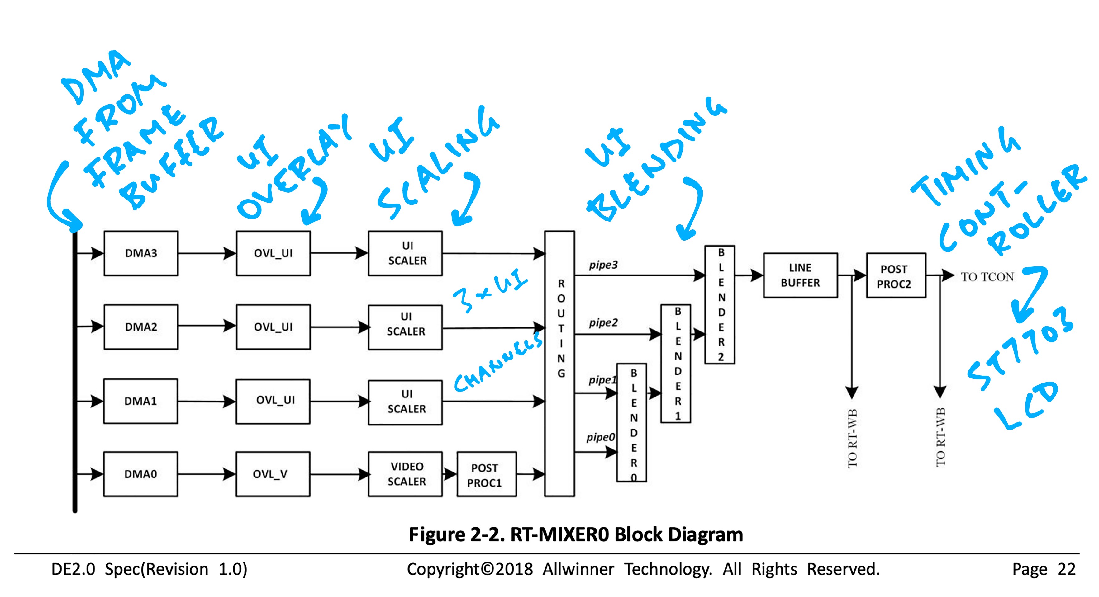
Real-Time Mixer in A64 Display Engine (Page 22)
Recall that Allwinner A64’s Display Engine is a Real-Time Mixer that handles real-time DMA, Overlay, Scaling and Blending of the Framebuffers…
And the Display Engine pushes the output pixels to the Timing Controller (TCON0) for display on PinePhone’s LCD Display.
The pic above shows how the Display Engine mixes together 3 UI Channels (Framebuffers) via DMA1, 2 and 3.
(Plus a Video Channel on DMA0, but we won’t use it today)
Is the Display Engine documented?
The official doc for the A64 Display Engine is here…
Though it doesn’t describe the actual steps for programming the Display Engine.
In a while we’ll boot Apache NuttX RTOS on PinePhone and experiment with the Display Engine, to understand it better.
(Overview of A64 Display Engine)
But the Display Engine doc doesn’t mention A64?
PinePhone’s A64 Display Engine is hidden under Allwinner H3 (page 22), because Allwinner A64 is actually a H3 upgraded with 64-bit Arm Cores…
“The A64 is basically an Allwinner H3 with the Cortex-A7 cores replaced with Cortex-A53 cores (ARM64 architecture). They share most of the memory map, clocks, interrupts and also uses the same IP blocks.”
Why are there 2 Mixers in the A64 Display Engine?
Maybe because A64 (or H3) was designed for OTT Set-Top Boxes with Picture-In-Picture Overlay Video?
The 3 UI Overlay Channels would be super helpful for overlaying an OTT Graphical UI on top of a Video Channel.
(Wait… Wasn’t Pine64 created thanks to OTT Boxes? 🤔)
(DE2TCON_MUX at Page 26 says that Mixer 0 is for TCON0 MIPI DSI, Mixer 1 for TCON1 HDMI Output)
How do we program the A64 Display Engine to render graphics?
Let’s begin by rendering simple Colour Blocks on the PinePhone Display…
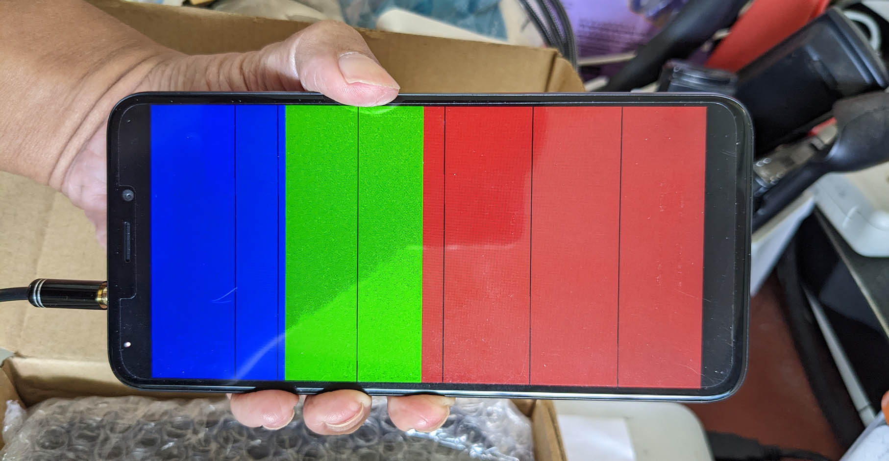
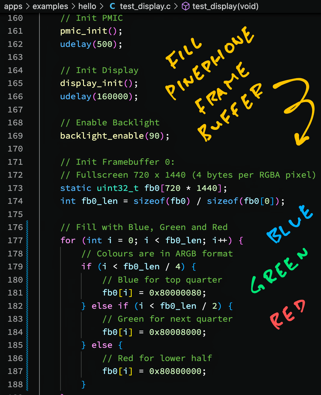
First we allocate the Framebuffer: test_display.c
// Init Framebuffer 0:
// Fullscreen 720 x 1440 (4 bytes per ARGB pixel)
// fb0_len is 720 * 1440
static uint32_t fb0[720 * 1440];
int fb0_len = sizeof(fb0) / sizeof(fb0[0]);
(PinePhone’s display resolution is 720 x 1440)
Each Pixel occupies 4 bytes. (ARGB 8888 Format)
Then we fill the Framebuffer with Blue, Green and Red: test_display.c
// Fill with Blue, Green and Red
for (int i = 0; i < fb0_len; i++) {
  // Colours are in ARGB format
  if (i < fb0_len / 4) {
    // Blue for top quarter
    fb0[i] = 0x80000080;
  } else if (i < fb0_len / 2) {
    // Green for next quarter
    fb0[i] = 0x80008000;
  } else {
    // Red for lower half
    fb0[i] = 0x80800000;
  }
}
Each Pixel in the Framebuffer is stored as 32-bit ARGB 8888.
Thus 0x8000 8000 means Semi-Transparent Green…
| Channel | Value |
|---|---|
| Alpha | 0x80 |
| Red | 0x00 |
| Green | 0x80 |
| Blue | 0x00 |
A64 Display Engine lets us render 3 Framebuffers as 3 UI Channels.
This is how we allocate the 3 UI Channels: test_display.c
// Allocate 3 UI Channels
static struct display disp;
memset(&disp, 0, sizeof(disp));
struct display *d = &disp;(display struct is defined here)
We point the First UI Channel to our Framebuffer: test_display.c
// Init UI Channel 1: (Base Channel)
// Fullscreen 720 x 1440
d->planes[0].fb_start = (uintptr_t) fb0;  // Framebuffer Address
d->planes[0].fb_pitch = 720 * 4;  // Framebuffer Pitch
d->planes[0].src_w    = 720;   // Source Width
d->planes[0].src_h    = 1440;  // Source Height
d->planes[0].dst_w    = 720;   // Dest Width
d->planes[0].dst_h = 1440; // Dest Height(fb_pitch is the number of bytes per row of pixels)
We disable the Second and Third UI Channels for now: test_display.c
// Init UI Channel 2: (First Overlay)
// Disable Channel for now
d->planes[1].fb_start = 0;

// Init UI Channel 3: (Second Overlay)
// Disable Channel for now
d->planes[2].fb_start = 0;

// Render the UI Channels over DMA
display_commit(d);
And we render the 3 UI Channels.
(display_commit is defined in the p-boot Display Code, we’ll come back to this)
That’s all! We should see the Blue, Green and Red Blocks like in the pic above.
(Not sure why there are black lines, needs investigation)
Didn’t we set the Alpha Channel to 0x80?
UI Channel 1 is the Base UI Channel, so the Alpha Channel has no effect.
(Actually UI Channel 1 is configured as XRGB 8888)
In a while we’ll set the Alpha Channels for UI Channels 2 and 3. And the UI Channels will appear as semi-transparent overlays.
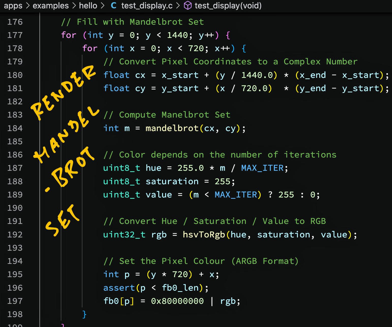
Colour Blocks are so blah. Are we sure we can render every single pixel correctly?
Let’s render something infinitely more detailed and sophisticated… Mandelbrot Set!

Earlier we created a Fullscreen Framebuffer: test_display.c
// Init Framebuffer 0:
// Fullscreen 720 x 1440 (4 bytes per ARGB pixel)
// fb0_len is 720 * 1440
static uint32_t fb0[720 * 1440];
int fb0_len = sizeof(fb0) / sizeof(fb0[0]);
Now we fill the Framebuffer with the Mandelbrot Set, pixel by pixel: test_display.c
// Fill with Mandelbrot Set.
// For every pixel row...
for (int y = 0; y < 1440; y++) {

  // For every pixel column...
  for (int x = 0; x < 720; x++) {

    // Convert Pixel Coordinates to a Complex Number
    float cx = x_start + (y / 1440.0) * (x_end - x_start);
    float cy = y_start + (x / 720.0)  * (y_end - y_start);

    // Compute Manelbrot Set
    int m = mandelbrot(cx, cy);

    // Color depends on the number of iterations.
    // MAX_ITER is 80
    uint8_t hue = 255.0 * m / MAX_ITER;
    uint8_t saturation = 255;
    uint8_t value = (m < MAX_ITER) ? 255 : 0;

    // Convert Hue / Saturation / Value to RGB
    uint32_t rgb = hsvToRgb(hue, saturation, value);

    // Set the Pixel Colour (ARGB Format)
    int p = (y * 720) + x;
    assert(p < fb0_len);
    fb0[p] = 0x80000000 | rgb;
  }
}(mandelbrot and hsvToRgb are defined here)
Then we initialise the 3 UI Channels and render them. (Like this)
The Mandelbrot Set appears on PinePhone, like in the pic above.
Yep we can render every single pixel precisely on PinePhone!
Earlier we said that updates to the Framebuffer are instantly pushed to PinePhone’s Display via DMA…
Can we prove it?
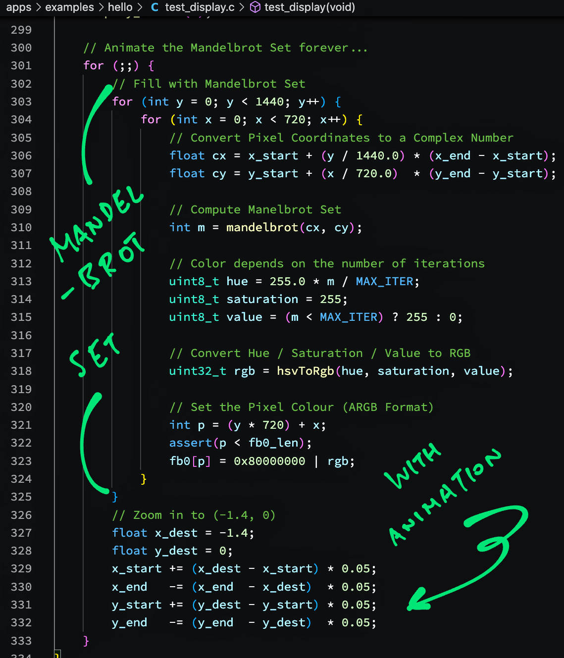
Yep let’s animate the Mandelbrot Set in our Framebuffer. And watch the updates appear instantly on PinePhone’s Display, thanks to Direct Memory Access (DMA)!
This is how we animate the Mandelbrot Set: test_display.c
// Omitted: Init UI Channels 1, 2 and 3
d->planes[0].fb_start = ...
d->planes[1].fb_start = ...
d->planes[2].fb_start = ...
...

// Render the UI Channels over DMA
display_commit(d);

// Animate the Mandelbrot Set forever.
// For every frame of animation...
for (;;) {

  // Fill with Mandelbrot Set.
  // For every pixel row...
  for (int y = 0; y < 1440; y++) {

    // For every pixel column...
    for (int x = 0; x < 720; x++) {
In the code above, we repeatly render the Mandelbrot Set for every frame of animation.
We render each frame the exact same way as before…
      // Convert Pixel Coordinates to a Complex Number
      float cx = x_start + (y / 1440.0) * (x_end - x_start);
      float cy = y_start + (x / 720.0)  * (y_end - y_start);

      // Compute Manelbrot Set
      int m = mandelbrot(cx, cy);

      // Color depends on the number of iterations
      // MAX_ITER is 80
      uint8_t hue = 255.0 * m / MAX_ITER;
      uint8_t saturation = 255;
      uint8_t value = (m < MAX_ITER) ? 255 : 0;

      // Convert Hue / Saturation / Value to RGB
      uint32_t rgb = hsvToRgb(hue, saturation, value);

      // Set the Pixel Colour (ARGB Format)
      int p = (y * 720) + x;
      assert(p < fb0_len);
      fb0[p] = 0x80000000 | rgb;
    }
  }
But now we tweak slightly the position of the Mandelbrot Set…
  // Zoom in to (-1.4, 0)
  float x_dest = -1.4;
  float y_dest = 0;
  x_start += (x_dest - x_start) * 0.05;
  x_end   -= (x_end  - x_dest)  * 0.05;
  y_start += (y_dest - y_start) * 0.05;
  y_end   -= (y_end  - y_dest)  * 0.05;
}
Before looping back to render the next frame.
We should see this Animated Mandelbrot Set…
Thus DMA works correctly for rendering our Framebuffers on the fly!
We don’t call display_commit after every frame?
display_commit only needs to be called once. It configures the Display Engine to read our Framebuffer directly via DMA.
Subsequent updates to the Framebuffer will be automatically pushed to the display over DMA.
Earlier we said that A64 Display Engine can render Framebuffers as Overlays. How can we do it?
The pic below shows that A64 Display Engine can render 3 Framebuffers (UI Channels) as overlays, via DMA1, 2 and 3…

Real-Time Mixer in A64 Display Engine (Page 22)
(Skipping DMA0 because it’s for Video only)
The UI Channels are rendered as overlays in a specific sequence (pic above)…
UI Channel 2 (DMA2) is rendered on top of UI Channel 1 (DMA1), then…
UI Channel 3 (DMA3) is rendered on top of UI Channel 2 (DMA2)
Our Mandelbrot Set is rendered on UI Channel 1 (DMA1), which is the Base Channel.
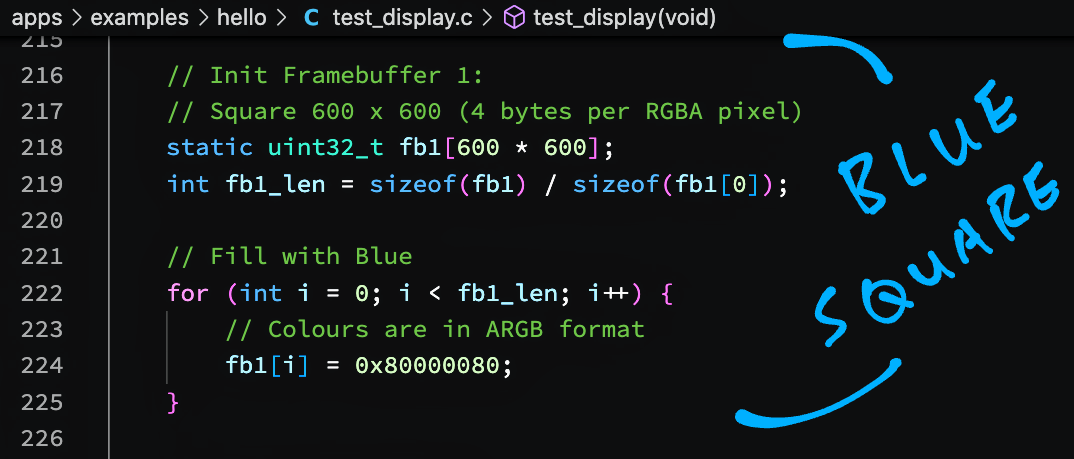
Let’s overlay a Blue Square on UI Channel 2 (DMA2).
First we prepare a 600 x 600 Framebuffer that contains a Semi-Transparent Blue Square: test_display.c
// Init Framebuffer 1:
// Square 600 x 600 (4 bytes per ARGB pixel)
// fb1_len is 600 * 600
static uint32_t fb1[600 * 600];
int fb1_len = sizeof(fb1) / sizeof(fb1[0]);

// Fill with Semi-Transparent Blue
for (int i = 0; i < fb1_len; i++) {
  // Colours are in ARGB format
  fb1[i] = 0x80000080;
}
The new Framebuffer is a little smaller than the Screen Width. (600 pixels vs 720 pixels)
Thanks to Framebuffer Blending in A64 Display Engine, it’s perfectly OK to render the new Framebuffer at 600 x 600. (As a partial screen region).
This is how we set UI Channel 2 to the 600 x 600 Framebuffer: test_display.c
// Init UI Channel 2: (First Overlay)
// Square 600 x 600
d->planes[1].fb_start = (uintptr_t) fb1;  // Framebuffer Address
d->planes[1].fb_pitch = 600 * 4;  // Framebuffer Pitch
d->planes[1].src_w    = 600;  // Source Width
d->planes[1].src_h    = 600;  // Source Height
d->planes[1].dst_w    = 600;  // Dest Width
d->planes[1].dst_h    = 600;  // Dest Height
d->planes[1].dst_x    = 52;   // Dest X Offset
d->planes[1].dst_y    = 52;   // Dest Y Offset
Can the Dest Width / Height be different from the Source Width / Height?
Yes, because the Display Engine supports Scaling. But we won’t do that today, to simplify our discussion.
Before we watch the outcome, let’s render another overlay…
Our PinePhone UI Overlay Sandwich has these goodies inside…
UI Channel 1: Mandelbrot Set (Base Channel)
UI Channel 2: Semi-Transparent Blue Square
Let’s top off our Cucumber Sandwich…
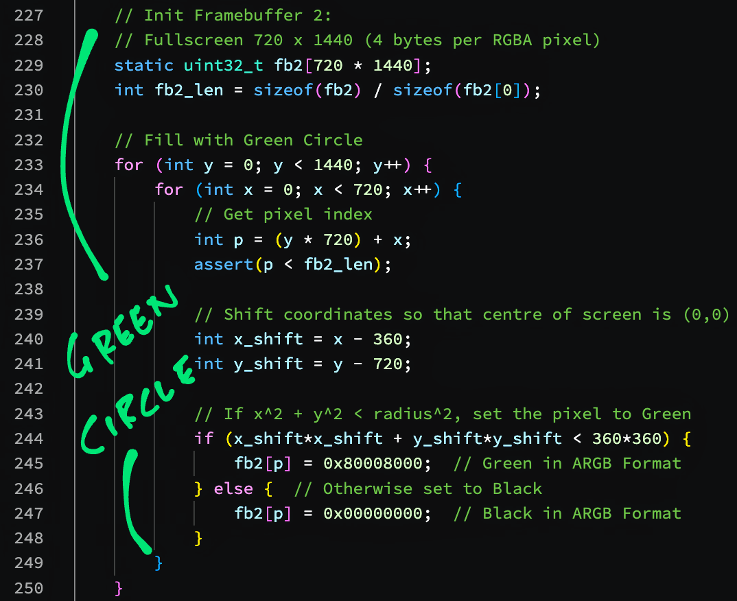
First we fill a Fullscreen Framebuffer with a Semi-Transparent Green Circle: test_display.c
// Init Framebuffer 2:
// Fullscreen 720 x 1440 (4 bytes per ARGB pixel)
// fb2_len is 720 * 1440
static uint32_t fb2[720 * 1440];
int fb2_len = sizeof(fb2) / sizeof(fb2[0]);

// Fill with Semi-Transparent Green Circle.
// For every pixel row...
for (int y = 0; y < 1440; y++) {

  // For every pixel column...
  for (int x = 0; x < 720; x++) {

    // Get pixel index
    int p = (y * 720) + x;
    assert(p < fb2_len);

    // Shift coordinates so that centre of screen is (0,0)
    int x_shift = x - 360;
    int y_shift = y - 720;

    // If pixel is inside circle (x^2 + y^2 < radius^2)...
    // Set the pixel to Semi-Transparent Green
    if (x_shift*x_shift + y_shift*y_shift < 360*360) {
      fb2[p] = 0x80008000;  // Semi-Transparent Green in ARGB Format
    } else {  // Otherwise set to Transparent Black
      fb2[p] = 0x00000000;  // Transparent Black in ARGB Format
    }
  }
}
Note that pixels outside the circle are set to Transparent Black.
(Which makes them invisible)
Next we point UI Channel 3 to the Fullscreen Framebuffer: test_display.c
// Init UI Channel 3: (Second Overlay)
// Fullscreen 720 x 1440 with Alpha Blending
d->planes[2].fb_start = (uintptr_t) fb2;  // Framebuffer Address
d->planes[2].fb_pitch = 720 * 4;  // Framebuffer Pitch
d->planes[2].src_w    = 720;   // Source Width
d->planes[2].src_h    = 1440;  // Source Height
d->planes[2].dst_w    = 720;   // Dest Width
d->planes[2].dst_h    = 1440;  // Dest Height
d->planes[2].dst_x    = 0;     // Dest X
d->planes[2].dst_y    = 0;     // Dest Y
d->planes[2].alpha    = 128;   // Dest Alpha
Note that we set the Destination Alpha for the entire UI Channel. So our Green Circle will appear super transparent.
Finally we render the 3 UI Channels…
// Render the UI Channels over DMA
display_commit(d);
We should see the Animated Mandelbrot Set, with Blue Square and (very faint) Green Circle as Overlays. (Pic below)
That’s how we render 3 UI Channels (with overlay blending) on PinePhone’s Display Engine!
(Why the horizontal lines in the Blue Square and Green Circle?)
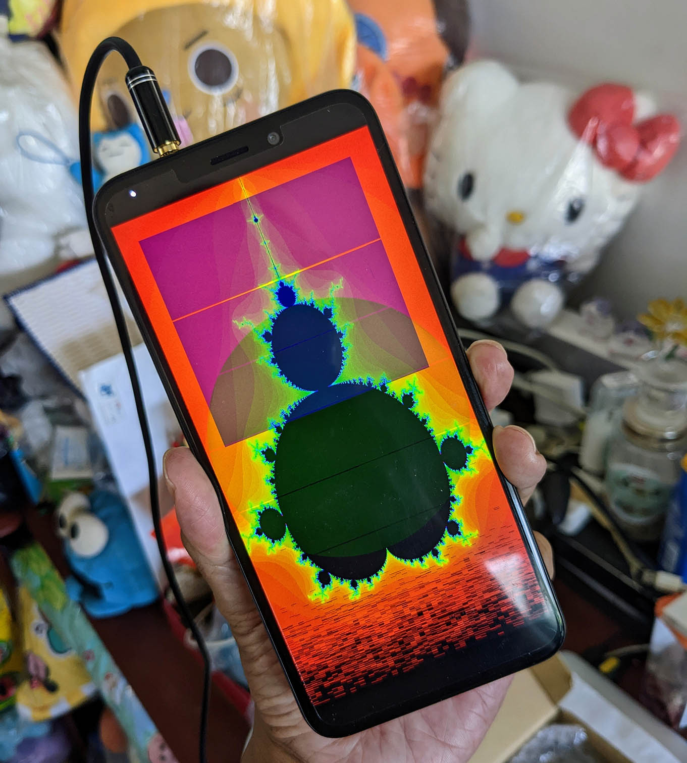
Mandelbrot Set with Blue Square and Green Circle as Overlays
We’ve seen the Test Code for Display Engine… How do we run the code?
To test the A64 Display Engine, we’ll boot Apache NuttX RTOS on PinePhone and run our Test App…
Follow these steps to download NuttX RTOS (with our Test App inside) to a microSD Card…
Connect our computer to PinePhone via a USB Serial Debug Cable. (At 115.2 kbps)
Boot PinePhone with NuttX RTOS in the microSD Card.
(NuttX won’t disturb the eMMC Flash Memory)
At the NuttX Shell, enter this command to run our Test App…
helloOur Test App controls the A64 Display Engine by setting the Hardware Registers (for the 3 UI Channels)…
HELLO NUTTX ON PINEPHONE!
...
Shell (NSH) NuttX-11.0.0-RC2
nsh> hello
...
display_commit
Configure Blender
  BLD BkColor:     0x1101088 = 0xff000000
  BLD Premultiply: 0x1101084 = 0x0
Channel 1: Set Overlay ...
Channel 1: Set Blender Output ...
Channel 1: Set Blender Input Pipe 0 ...
Channel 1: Disable Scaler ...
Channel 2: Set Overlay ...
Channel 2: Set Blender Input Pipe 1 ...
Channel 2: Disable Scaler ...
Channel 3: Set Overlay ...
Channel 3: Set Blender Input Pipe 2 ...
Channel 3: Disable Scaler ...
Set BLD Route and BLD FColor Control
  BLD Route:          0x1101080 = 0x321
  BLD FColor Control: 0x1101000 = 0x701
Apply Settings
GLB DBuff: 0x1100008 = 0x1And the Mandelbrot Set appears on PinePhone, together with the Blue Square and Green Circle as overlays. (Pic above)
Yep we have successfully tested the A64 Display Engine on PinePhone! 🎉
Hmmm building the Test Code looks complicated…
Yeah we need a few steps to build the Test Code because we patched together a few programs to make it work…
Apache NuttX RTOS for PinePhone
Zig Driver for MIPI Display Serial Interface
p-boot Display Code
The steps will be a lot simpler when we have completed the Display Engine Driver for NuttX.
Let’s talk about the p-boot Display Code…
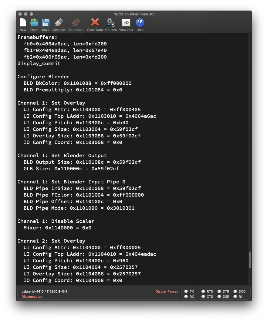
Running p-boot Display Code on Apache NuttX RTOS with logging
About the code that controls A64 Display Engine… Where is display_commit defined?
display_commit comes from the super-helpful p-boot PinePhone Bootloader project, which runs directly on PinePhone Hardware. (“Bare Metal”)
To test the A64 Display Engine on Apache NuttX RTOS, we borrowed these Source Files (relevant to the Display Engine) from p-boot…
(Plus a whole bunch of Header Files)
Then we modified the above files to compile on NuttX…
Which lets us experiment with the A64 Display Engine on NuttX.
How does it control the A64 Display Engine?
display_commit controls the A64 Display Engine by writing to the Hardware Registers for the Display Engine.
The Display Engine’s Hardware Registers are described here…
But what values does display_commit write to the Hardware Registers?
To find out how display_commit updates the Hardware Registers (while rendering the UI Channels), we modded the p-boot Display Code to log all Register Writes…
Which tells us all the Hardware Registers and their values…
Configure Blender
  BLD BkColor:     0x1101088 = 0xff000000
  BLD Premultiply: 0x1101084 = 0x0

Channel 1: Set Overlay
  UI Config Attr:      0x1103000 = 0xff000405
  UI Config Top LAddr: 0x1103010 = 0x4064a6ac
  UI Config Pitch:     0x110300c = 0xb40
  UI Config Size:      0x1103004 = 0x59f02cf
  UI Overlay Size:     0x1103088 = 0x59f02cf
  IO Config Coord:     0x1103008 = 0x0

Channel 1: Set Blender Output
  BLD Output Size: 0x110108c = 0x59f02cf
  GLB Size:        0x110000c = 0x59f02cf

Channel 1: Set Blender Input Pipe 0
  BLD Pipe InSize: 0x1101008 = 0x59f02cf
  BLD Pipe FColor: 0x1101004 = 0xff000000
  BLD Pipe Offset: 0x110100c = 0x0
  BLD Pipe Mode:   0x1101090 = 0x3010301

Channel 1: Disable Scaler
  Mixer: 0x1140000 = 0x0

Channel 2: ...When we study the log, we’ll understand how we should program the A64 Display Engine to render the 3 UI Channels.
Our findings are documented here…
This is very helpful as we create the NuttX Display Driver for PinePhone…
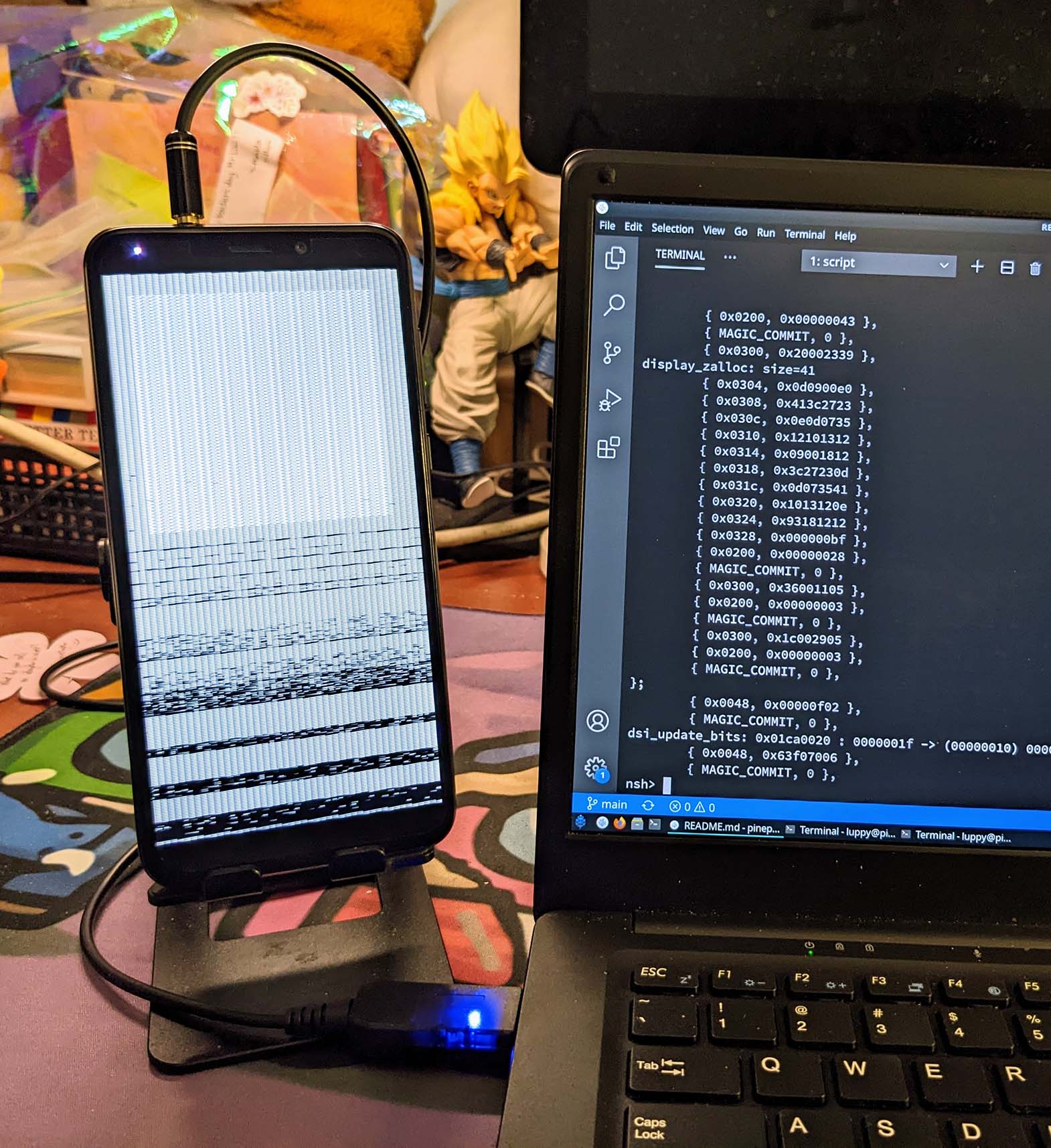
Testing the NuttX Display Driver for PinePhone
Once again, why are we doing all this?
We’re now porting Apache NuttX RTOS to PinePhone.
Someday we hope to have a fully-functional PinePhone running on NuttX RTOS…
(Or maybe just run PinePhone on NuttX as a simple touchscreen gadget)
To do that, we need a NuttX Display Driver.
That’s why we’re probing the internals of PinePhone, to learn everything we need to build the driver.
We’ve documented our earlier research on PinePhone’s MIPI Display Serial Interface…
Today we learnt so much about PinePhone’s A64 Display Engine…
We’re all set to build the NuttX Display Driver for PinePhone!
Is there a specific sequence of steps for calling the Display Serial Interface, Display Engine and Timing Controller?
To render graphics on PinePhone’s LCD Display, our Display Driver needs to follow these steps…
How shall we build the PinePhone Display Driver?
We’ll create the PinePhone Display Driver based on the NuttX Driver for Sitronix ST7789…
That’s because ST7789 is somewhat similar to PinePhone’s ST7703 LCD Controller.
But ST7789 doesn’t support Framebuffers?
Yeah for PinePhone we’ll wrap the A64 DMA Framebuffers with this interface for NuttX Framebuffers…
And we might get inspired by this implementation of Display Overlays in the STM32 LCD TFT Display Controller (LTDC)…
We have started the Zig Implementation of the NuttX Driver (for MIPI Display Serial Interface)…
We’ll add the A64 Display Engine in the next article!
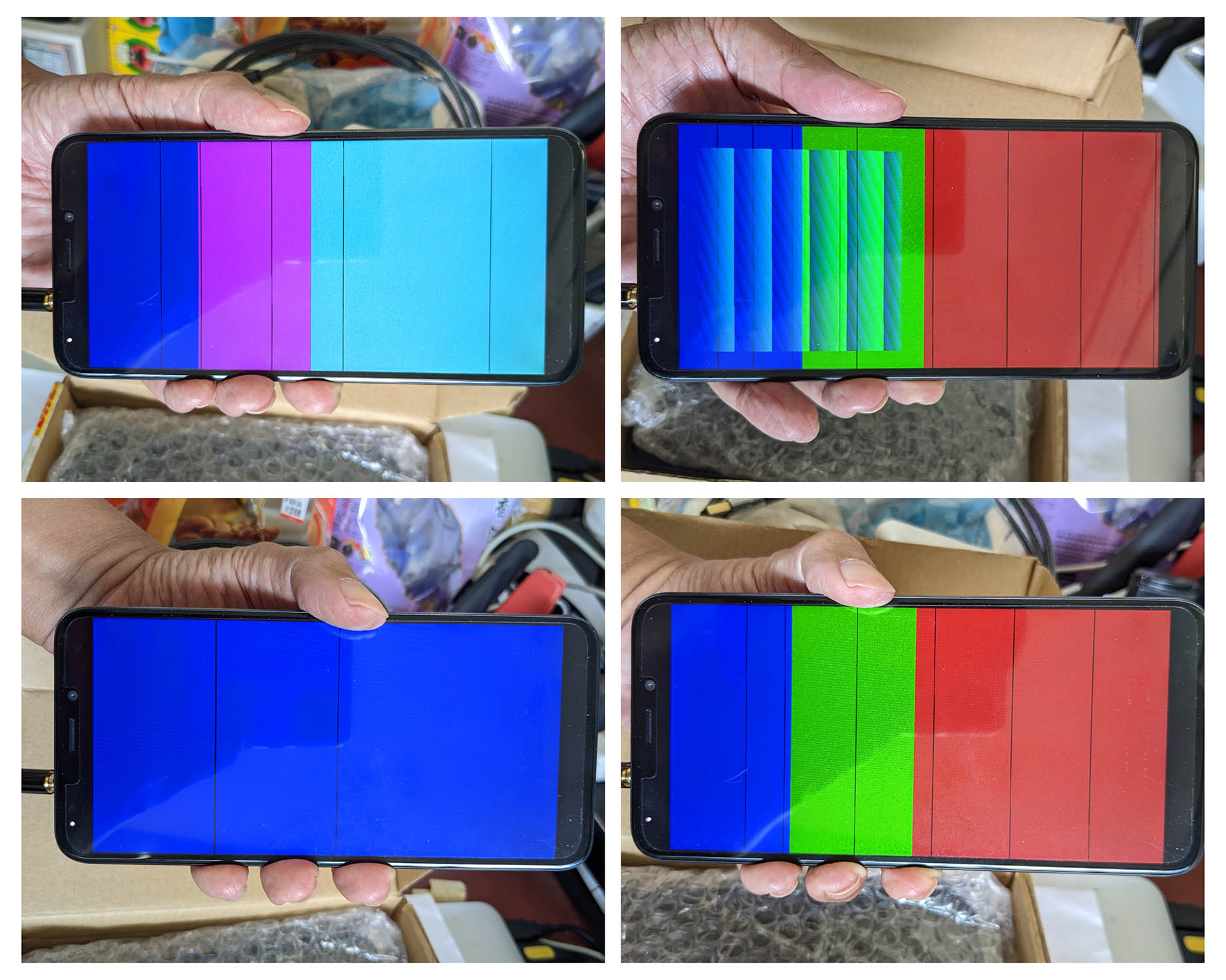
I hope we learnt lots today about Display Rendering on PinePhone…
What’s the Display Engine (DE) inside PinePhone
How the Timing Controller (TCON0) controls PinePhone’s LCD Display
How we call DE and TCON0 to render graphics
How our new PinePhone Display Driver will support DE and TCON0
Please join me in the next article as we create the PinePhone Display Engine Driver for Apache NuttX RTOS!
“NuttX RTOS for PinePhone: Render Graphics in Zig” Please check out the other articles on NuttX for PinePhone…
Many Thanks to my GitHub Sponsors for supporting my work! This article wouldn’t have been possible without your support.
Got a question, comment or suggestion? Create an Issue or submit a Pull Request here…

Display Engine (DE) and Timing Controller (TCON0) from A64 User Manual (Page 498)
The official doc for the Allwinner A64 Display Engine is here…
PinePhone’s A64 Display Engine is hidden under Allwinner H3 (page 22), because Allwinner A64 is actually a H3 upgraded with 64-bit Arm Cores.
(Also check out this DE2 Register Guide)
Earlier we said that Allwinner A64’s Display Engine is a Real-Time Mixer that handles real-time DMA, Overlay, Scaling and Blending of the Framebuffers…
And the Display Engine pushes the output pixels to the Timing Controller (TCON0) for display on PinePhone’s LCD Display…
According to the doc, the Display Engine Base Address is 0x0100 0000 (DE Page 24)
What’s a Display Engine Mixer?
DE RT-MIXER: (DE Page 87)
“The RT-mixer Core consist of dma, overlay, scaler and blender block. It supports 4 layers overlay in one pipe, and its result can scaler up or down to blender in the next processing.”
The Display Engine has 2 Mixers: RT-MIXER0 and RT-MIXER1.
DE RT-MIXER0 has 4 Channels (DE Offset 0x10 0000, DE Page 87)
Channel 0 for Video
(DMA0, Video Overlay, Video Scaler)
Channels 1, 2 and 3 for UI
(DMA1 / 2 / 3, 3 x UI Overlays, 3 x UI Scalers, 3 x UI Blenders)
4 Overlay Layers per Channel
(We only use 1 Overlay Layer per Channel)
Layer Priority is Layer 3 > Layer2 > Layer 1 > Layer 0 (DE Page 89)
Our Display Engine Demo configures the 4 Channels as follows…
Channel 0 is unused
(No video right now)
Channel 1 has Pixel Format XRGB 8888
(Alpha Channel is disabled)
Channels 2 and 3 have Pixel Format ARGB 8888
(Alpha Channel is enabled)
Hardware Registers for RT-MIXER0 (DE Page 90)…
| Hardware Register | RT-MIXER0 Offset |
|---|---|
| GLB (Global Registers) | 0x00 0000 |
| BLD (Blender) | 0x00 1000 |
| OVL_V(CH0) (Video Overlay / Channel 0) | 0x00 2000 |
| OVL_UI(CH1) (UI Overlay / Channel 1) | 0x00 3000 |
| OVL_UI(CH2) (UI Overlay / Channel 2) | 0x00 4000 |
| OVL_UI(CH3) (UI Overlay / Channel 3) | 0x00 5000 |
| VIDEO_SCALER(CH0) (Video Scaler / Channel 0) | 0x02 0000 |
| UI_SCALER1(CH1) (UI Scaler / Channel 1) | 0x04 0000 |
| UI_SCALER2(CH2) (UI Scaler / Channel 2) | 0x05 0000 |
| UI_SCALER3(CH3) (UI Scaler / Channel 3) | 0x06 0000 |
| POST_PROC1 (Post Processor 1) | 0x0A 0000 |
| POST_PROC2 (Post Processor 2) | 0x0B 0000 |
| DMA (Direct Memory Access) | 0x0C 0000 |
The pic below shows how DE RT-MIXER0 mixes together 3 UI Channels (Framebuffers) via DMA1, 2 and 3 (plus a Video Channel on DMA0)…

Real-Time Mixer in A64 Display Engine (Page 22)
DE RT-MIXER1 has 2 Channels (DE Offset 0x20 0000, DE Page 23)
Channel 0 for Video
(DMA0, Video Overlay, Video Scaler)
Channel 1 for UI
(DMA1, UI Overlay, UI Scaler, UI Blender)
(We don’t use RT-MIXER1 right now)
RT-MIXER0 and RT-MIXER1 are multiplexed to Timing Controller TCON0. (Like this)
TCON0 is connected to PinePhone’s ST7703 LCD Controller over MIPI Display Serial Interface. (See this)
Hence RT-MIXER0 mixes 1 Video Channel with 3 UI Channels over DMA. And pumps the pixels continuously to ST7703 LCD Controller. (Via the Timing Controller TCON0)
In today’s demo we used the 3 UI Channels to render (pic below)…
In the following chapters we explain how the 3 UI Channels were initialised and rendered by setting the Hardware Registers for A64 Display Engine…

Mandelbrot Set with Blue Square and Green Circle as Overlays
We won’t use these Display Engine Features today…
DE RT-WB (Write-Back Controller): (DE Page 116)
“The Real-time write-back controller (RT-WB) provides data capture function for display engine. It captures data from RT-mixer module, performs the image resizing function, and then write-back to SDRAM.”
(For screen capture?)
DE VSU (Video Scaler): (DE Page 128)
“The Video Scaler (VS) provides YUV format image resizing function for display engine. It receives data from overlay module, performs the image resizing function, and outputs to video post-processing modules.”
DE Rotation: (DE Page 137)
“There are several types of rotation: clockwise 0/90/180/270 degree Rotation and H-Flip/V-Flip. Operation of Copy is the same as a 0 degree rotation.”
Nope to these too…
How do we initialise PinePhone’s Allwinner A64 Display Engine at startup?
As deciphered from the following logs…
(Captured from p-boot de2_init)
(Captured from p-boot clock_set_pll_de)
Below are the steps to initialise the Allwinner A64 Display Engine at startup…
Set High Speed SRAM to DMA Mode
Set BIST_DMA_CTRL_SEL to 0 for DMA (DMB)
BIST_DMA_CTRL_SEL (Bist and DMA Control Select) is Bit 0 of SRAM_CTRL_REG1
SRAM_CTRL_REG1 (SRAM Control Register 1) is at SRAM Registers Offset 0x4
SRAM Registers Base Address is 0x01C0 0000
Set SRAM for video use
  0x1c0 0004 = 0x0 (DMB)
Set Display Engine PLL to 297 MHz
Set PLL_DE_CTRL_REG to 0x8100 1701 (DMB)
PLL_ENABLE (Bit 31) = 1 (Enable PLL)
PLL_MODE_SEL (Bit 24) = 1 (Integer Mode)
PLL_FACTOR_N (Bits 8 to 14) = 23 (N = 24)
PLL_PRE_DIV_M (Bits 0 to 3) = 1 (M = 2)
Actual PLL Output = 24 MHz * N / M = 288 MHz
(Slighltly below 297 MHz due to truncation)
PLL_DE_CTRL_REG (PLL Display Engine Control Register) is at CCU Offset 0x0048
CCU (Clock Control Unit) Base Address is 0x01C2 0000
Setup DE2 PLL
  clock_set_pll_de: clk=297000000
  PLL10 rate = 24000000 * n / m
  0x1c2 0048 = 0x8100 1701 (DMB)
Wait for Display Engine PLL to be stable
Poll PLL_DE_CTRL_REG (from above) until LOCK (Bit 28) is 1
(PLL is Locked and Stable)
Setup DE2 PLL
  while (!(readl(0x1c2 0048) & 0x1000 0000))
Set Special Clock to Display Engine PLL
Clear DE_CLK_REG bits 0x0300 0000
Set DE_CLK_REG bits 0x8100 0000
SCLK_GATING (Bit 31) = 1 (Enable Special Clock)
CLK_SRC_SEL (Bits 24 to 26) = 1 (Clock Source is Display Engine PLL)
DE_CLK_REG (Display Engine Clock Register) is at CCU Offset 0x0104
CCU (Clock Control Unit) Base Address is 0x01C2 0000
Enable DE2 special clock
  clrsetbits 0x1c2 0104, 0x300 0000, 0x8100 0000
Enable AHB (AMBA High-speed Bus) for Display Engine: De-Assert Display Engine
Set BUS_SOFT_RST_REG1 bits 0x1000
DE_RST (Bit 12) = 1 (De-Assert Display Engine)
BUS_SOFT_RST_REG1 (Bus Software Reset Register 1) is at CCU Offset 0x02C4
CCU (Clock Control Unit) Base Address is 0x01C2 0000
Enable DE2 ahb
  setbits 0x1c2 02c4, 0x1000
Enable AHB (AMBA High-speed Bus) for Display Engine: Pass Display Engine
Set BUS_CLK_GATING_REG1 bits 0x1000
DE_GATING (Bit 12) = 1 (Pass Display Engine)
BUS_CLK_GATING_REG1 (Bus Clock Gating Register 1) is at CCU Offset 0x0064
CCU (Clock Control Unit) Base Address is 0x01C2 0000
Enable DE2 ahb
  setbits 0x1c2 0064, 0x1000
Enable Clock for MIXER0: SCLK Clock Pass
Set SCLK_GATE bits 0x1
CORE0_SCLK_GATE (Bit 0) = 1 (Clock Pass)
SCLK_GATE is at DE Offset 0x000
Display Engine (DE) Base Address is 0x0100 0000
Enable clock for mixer 0, set route MIXER0->TCON0
  setbits 0x100 0000, 0x1
Enable Clock for MIXER0: HCLK Clock Reset Off
Set AHB_RESET bits 0x1
CORE0_HCLK_RESET (Bit 0) = 1 (Reset Off)
AHB_RESET is at DE Offset 0x008
Display Engine (DE) Base Address is 0x0100 0000
Enable clock for mixer 0, set route MIXER0->TCON0
  setbits 0x100 0008, 0x1
Enable Clock for MIXER0: HCLK Clock Pass
Set HCLK_GATE bits 0x1
CORE0_HCLK_GATE (Bit 0) = 1 (Clock Pass)
HCLK_GATE is at DE Offset 0x004
Display Engine (DE) Base Address is 0x0100 0000
Enable clock for mixer 0, set route MIXER0->TCON0
  setbits 0x100 0004, 0x1
Route MIXER0 to TCON0
Clear DE2TCON_MUX bits 0x1
DE2TCON_MUX (Bit 0) = 0
(Route MIXER0 to TCON0; Route MIXER1 to TCON1)
DE2TCON_MUX is at DE Offset 0x010
Display Engine (DE) Base Address is 0x0100 0000
Enable clock for mixer 0, set route MIXER0->TCON0
  clrbits 0x100 0010, 0x1
Clear MIXER0 Registers: Global Registers (GLB), Blender (BLD), Video Overlay (OVL_V), UI Overlay (OVL_UI)
Set MIXER0 Offsets 0x0000 - 0x5FFF to 0
Which covers…
GLB (Global Regisers) at MIXER0 Offset 0x0000
BLD (Blender) at MIXER0 Offset 0x1000
OVL_V(CH0) (Video Overlay) at MIXER0 Offset 0x2000
OVL_UI(CH1) (UI Overlay 1) at MIXER0 Offset 0x3000
OVL_UI(CH2) (UI Overlay 2) at MIXER0 Offset 0x4000
OVL_UI(CH3) (UI Overlay 3) at MIXER0 Offset 0x5000
MIXER0 is at DE Offset 0x0010 0000
Display Engine (DE) Base Address is 0x0100 0000
Clear all registers
  0x110 0000 to 0x110 5fff = 0x0
Disable MIXER0 Modules…
Set to 0 the following registers…
VS_CTRL_REG at VIDEO_SCALER(CH0) Offset 0
EN (Bit 0) = 0 (Disable Video Scaler)
TODO: 0x113 0000 is Undocumented
(Is there a mixup with UI_SCALER3?)
UIS_CTRL_REG at UI_SCALER1(CH1) Offset 0
EN (Bit 0) = 0 (Disable UI Scaler)
UIS_CTRL_REG at UI_SCALER2(CH2) Offset 0
EN (Bit 0) = 0 (Disable UI Scaler)
TODO: Missing UI_SCALER3(CH3) at MIXER0 Offset 0x06 0000
(Is there a mixup with 0x113 0000 above?)
GCTRL_REG(FCE) at FCE Offset 0
EN (Bit 0) = 0 (Disable FCE)
GCTRL_REG(BWS) at BWS Offset 0
EN (Bit 0) = 0 (Disable BWS)
LTI_CTL at LTI Offset 0
LTI_EN (Bit 0) = 0 (Close LTI)
LP_CTRL_REG at PEAKING Offset 0
EN (Bit 0) = 0 (Disable PEAKING)
ASE_CTL_REG at ASE Offset 0
ASE_EN (Bit 0) = 0 (Disable ASE)
FCC_CTL_REG at FCC Offset 0
Enable (Bit 0) = 0 (Disable FCC)
GNECTL_REG at DRC Offset 0
BIST_EN (Bit 0) = 0 (Disable BIST)
Offsets of the above registers…
VIDEO_SCALER(CH0) is at MIXER0 Offset 0x02 0000
UI_SCALER1(CH1) is at MIXER0 Offset 0x04 0000
UI_SCALER2(CH2) is at MIXER0 Offset 0x05 0000
FCE is at MIXER0 Offset 0x0A 0000
BWS is at MIXER0 Offset 0x0A 2000
LTI is at MIXER0 Offset 0x0A 4000
PEAKING is at MIXER0 Offset 0x0A 6000
ASE is at MIXER0 Offset 0x0A 8000
FCC is at MIXER0 Offset 0x0A A000
DRC is at Address 0x011B 0000
MIXER0 is at DE Offset 0x0010 0000
Display Engine (DE) Base Address is 0x0100 0000
Clear all registers
  0x112 0000 = 0x0
  0x113 0000 = 0x0
  0x114 0000 = 0x0
  0x115 0000 = 0x0
  0x11a 0000 = 0x0
  0x11a 2000 = 0x0
  0x11a 4000 = 0x0
  0x11a 6000 = 0x0
  0x11a 8000 = 0x0
  0x11a a000 = 0x0
  0x11b 0000 = 0x0
Enable MIXER0
Set GLB_CTL to 1 (DMB)
EN (Bit 0) = 1 (Enable Mixer)
GLB_CTL is at MIXER0 Offset 0
MIXER0 is at DE Offset 0x0010 0000
Display Engine (DE) Base Address is 0x0100 0000
Enable mixer
  0x110 0000 = 0x1 (DMB)
We have implemented in Zig the above A64 Display Engine Initialisation…
We have converted the above Zig Driver to C and added to NuttX Kernel…

Running p-boot Display Code on Apache NuttX RTOS with logging
We’ve seen the Hardware Registers for the Allwinner A64 Display Engine…
And we need to program the Hardware Registers to create the NuttX Display Driver for PinePhone…
How will we program the Hardware Registers to render the UI Channels?
To find out how display_commit updates the Hardware Registers (while rendering the UI Channels), we modded the p-boot Display Code to log all Register Writes…
Which produces a log that tells us all the Hardware Registers and their values…
After studying the log, we have identified the steps to render the 3 UI Channels with the Display Engine.
This is how we’ll create a NuttX Driver for PinePhone’s A64 Display Engine that implements Display Rendering…
(Refer to Memory Mapping List and Register List at DE Page 90)
Set Blender Background and Pre-Multiply…
BLD_BK_COLOR (Blender Background Color) at BLD Offset 0x88
Set to 0xFF00 0000 (Black Background Color)
RESERVED (Bits 24 to 31) = 0xFF (Undocumented)
RED (Bits 16 to 23) = 0
GREEN (Bits 8 to 15) = 0
BLUE (Bits 0 to 7) = 0
BLD_PREMUL_CTL (Blender Pre-Multiply Control) at BLD Offset 0x84
Set to 0 (No Pre-Multiply for Alpha, Pipes 0 to 3)
P3_ALPHA_MODE (Bit 3) = 0 (Pipe 3: No Pre-Multiply)
P2_ALPHA_MODE (Bit 2) = 0 (Pipe 2: No Pre-Multiply)
P1_ALPHA_MODE (Bit 1) = 0 (Pipe 1: No Pre-Multiply)
P0_ALPHA_MODE (Bit 0) = 0 (Pipe 0: No Pre-Multiply)
Configure Blender
BLD BkColor:     0x110 1088 = 0xff00 0000
BLD Premultiply: 0x110 1084 = 0x0
For Channels 1 to 3…
If Channel is unused, disable Overlay, Pipe and Scaler. Skip to next Channel
OVL_UI_ATTR_CTL (UI Overlay Attribute Control) at OVL_UI Offset 0x00
Set to 0 (Disable UI Overlay Channel)
LAY_EN (Bit 0) = 0 (Disable Layer)
UIS_CTRL_REG at Offset 0 of UI_SCALER1(CH1) or UI_SCALER2(CH2) or UI_SCALER3(CH3)
Set to 0 (Disable UI Scaler)
EN (Bit 0) = 0 (Disable UI Scaler)
OVL_UI(CH1) (UI Overlay 1) is at MIXER0 Offset 0x3000
OVL_UI(CH2) (UI Overlay 2) is at MIXER0 Offset 0x4000
OVL_UI(CH3) (UI Overlay 3) is at MIXER0 Offset 0x5000
UI_SCALER1(CH1) is at MIXER0 Offset 0x04 0000
UI_SCALER2(CH2) is at MIXER0 Offset 0x05 0000
UI_SCALER3(CH3) is at MIXER0 Offset 0x06 0000
MIXER0 is at DE Offset 0x0010 0000
Display Engine (DE) Base Address is 0x0100 0000
Channel 2: Disable Overlay and Pipe
UI Config Attr: 0x110 4000 = 0x0

Channel 3: Disable Overlay and Pipe
UI Config Attr: 0x110 5000 = 0x0

Channel 2: Disable Scaler
Mixer: 0x115 0000 = 0x0

Channel 3: Disable Scaler
Mixer: 0x116 0000 = 0x0
Channel 1 has Pixel Format XRGB 8888:
OVL_UI_ATTR_CTL → LAY_FBFMT = 4
Channels 2 and 3 have Pixel Format ARGB 8888:
OVL_UI_ATTR_CTL → LAY_FBFMT = 0
Set Overlay (Assume Layer = 0)
OVL_UI_ATTR_CTL (UI Overlay Attribute Control) at OVL_UI Offset 0x00
For Channel 1: Set to 0xFF00 0405
For Channel 2: Set to 0xFF00 0005
For Channel 3: Set to 0x7F00 0005
LAY_GLBALPHA (Bits 24 to 31) = 0xFF or 0x7F
(Global Alpha Value is Opaque or Semi-Transparent)
LAY_FBFMT (Bits 8 to 12) = 4 or 0
(Input Data Format is XRGB 8888 or ARGB 8888)
LAY_ALPHA_MODE (Bits 1 to 2) = 2
(Global Alpha is mixed with Pixel Alpha)
(Input Alpha Value = Global Alpha Value * Pixel’s Alpha Value)
LAY_EN (Bit 0) = 1 (Enable Layer)
OVL_UI_TOP_LADD (UI Overlay Top Field Memory Block Low Address) at OVL_UI Offset 0x10
Set to Framebuffer Address: fb0, fb1 or fb2
OVL_UI_PITCH (UI Overlay Memory Pitch) at OVL_UI Offset 0x0C
Set to (width * 4), number of bytes per row
OVL_UI_MBSIZE (UI Overlay Memory Block Size) at OVL_UI Offset 0x04
Set to (height-1) << 16 + (width-1)
OVL_UI_SIZE (UI Overlay Overlay Window Size) at OVL_UI Offset 0x88
Set to (height-1) << 16 + (width-1)
OVL_UI_COOR (UI Overlay Memory Block Coordinate) at OVL_UI Offset 0x08
Set to 0 (Overlay at X=0, Y=0)
Channel 1: Set Overlay (fb0 is 720 x 1440)
UI Config Attr:      0x110 3000 = 0xff00 0405
UI Config Top LAddr: 0x110 3010 = 0x4064 a6ac (Address of fb0)
UI Config Pitch:     0x110 300c = 0xb40 (720 * 4)
UI Config Size:      0x110 3004 = 0x59f 02cf (1439 << 16 + 719)
UI Overlay Size:     0x110 3088 = 0x59f 02cf (1439 << 16 + 719)
IO Config Coord:     0x110 3008 = 0x0

Channel 2: Set Overlay (fb1 is 600 x 600)
UI Config Attr:      0x110 4000 = 0xff00 0005
UI Config Top LAddr: 0x110 4010 = 0x404e adac (Address of fb1)
UI Config Pitch:     0x110 400c = 0x960 (600 * 4)
UI Config Size:      0x110 4004 = 0x257 0257 (599 << 16 + 599)
UI Overlay Size:     0x110 4088 = 0x257 0257 (599 << 16 + 599)
IO Config Coord:     0x110 4008 = 0x0

Channel 3: Set Overlay (fb2 is 720 x 1440)
UI Config Attr:      0x110 5000 = 0x7f00 0005
UI Config Top LAddr: 0x110 5010 = 0x400f 65ac (Address of fb2)
UI Config Pitch:     0x110 500c = 0xb40 (720 * 4)
UI Config Size:      0x110 5004 = 0x59f 02cf (1439 << 16 + 719)
UI Overlay Size:     0x110 5088 = 0x59f 02cf (1439 << 16 + 719)
IO Config Coord:     0x110 5008 = 0x0
For Channel 1: Set Blender Output
BLD_SIZE (Blender Output Size Setting) at BLD Offset 0x08C
Set to (height-1) << 16 + (width-1)
GLB_SIZE (Global Size) at GLB Offset 0x00C
Set to (height-1) << 16 + (width-1)
Channel 1: Set Blender Output
BLD Output Size: 0x110 108c = 0x59f 02cf (1439 * 16 + 719)
GLB Size:        0x110 000c = 0x59f 02cf (1439 * 16 + 719)
Set Blender Input Pipe (N = Pipe Number, from 0 to 2 for Channels 1 to 3)
BLD_CH_ISIZE (Blender Input Memory Size) at BLD Offset 0x008 + N*0x10 (N=0,1,2,3,4)
Set to (height-1) << 16 + (width-1)
BLD_FILL_COLOR (Blender Fill Color) at BLD Offset 0x004 + N*0x10 (N=0,1,2,3,4)
Set to 0xFF00 0000 (Opaque Black)
ALPHA (Bits 24 to 31) = 0xFF
RED (Bits 16 to 23) = 0
GREEN (Bits 8 to 15) = 0
BLUE (Bits 0 to 7) = 0
BLD_CH_OFFSET (Blender Input Memory Offset) at BLD Offset 0x00C + N*0x10 (N=0,1,2,3,4)
Set to y_offset << 16 + x_offset
For Channel 1: Set to 0
For Channel 2: Set to 0x34 0034
For Channel 3: Set to 0
BLD_CTL (Blender Control) at BLD Offset 0x090 + N*4
Set to 0x301 0301
BLEND_AFD (Bits 24 to 27) = 3
(Coefficient for destination alpha data Q[d] is 1-A[s])
BLEND_AFS (Bits 16 to 19) = 1
(Coefficient for source alpha data Q[s] is 1)
BLEND_PFD (Bits 8 to 11) = 3
(Coefficient for destination pixel data F[d] is 1-A[s])
BLEND_PFS (Bits 0 to 3) = 1
(Coefficient for source pixel data F[s] is 1)
Note: DE Page 91 shows incorrect offset N*0x14 for BLD_CH_ISIZE, BLD_FILL_COLOR and BLD_CH_OFFSET. Correct offset is N*0x10, see DE Page 108
Channel 1: Set Blender Input Pipe 0 (fb0 is 720 x 1440)
BLD Pipe InSize: 0x110 1008 = 0x59f 02cf (1439 * 16 + 719)
BLD Pipe FColor: 0x110 1004 = 0xff00 0000
BLD Pipe Offset: 0x110 100c = 0x0
BLD Pipe Mode:   0x110 1090 = 0x301 0301

Channel 2: Set Blender Input Pipe 1 (fb1 is 600 x 600)
BLD Pipe InSize: 0x110 1018 = 0x257 0257 (599 << 16 + 599)
BLD Pipe FColor: 0x110 1014 = 0xff00 0000
BLD Pipe Offset: 0x110 101c = 0x34 0034
BLD Pipe Mode:   0x110 1094 = 0x301 0301

Channel 3: Set Blender Input Pipe 2 (fb2 is 720 x 1440)
BLD Pipe InSize: 0x110 1028 = 0x59f 02cf (1439 * 16 + 719)
BLD Pipe FColor: 0x110 1024 = 0xff00 0000
BLD Pipe Offset: 0x110 102c = 0x0
BLD Pipe Mode:   0x110 1098 = 0x301 0301
Disable Scaler (Assume we’re not scaling)
UIS_CTRL_REG at Offset 0 of UI_SCALER1(CH1) or UI_SCALER2(CH2) or UI_SCALER3(CH3)
Set to 0 (Disable UI Scaler)
EN (Bit 0) = 0 (Disable UI Scaler)
Channel 1: Disable Scaler
Mixer: 0x114 0000 = 0x0

Channel 2: Disable Scaler
Mixer: 0x115 0000 = 0x0

Channel 3: Disable Scaler
Mixer: 0x116 0000 = 0x0
Set Blender Route and Enable Blender Pipes
BLD_CH_RTCTL (Blender Routing Control) at BLD Offset 0x080
If Rendering 3 UI Channels: Set to 0x321 (DMB)
P2_RTCTL (Bits 8 to 11) = 3 (Pipe 2 from Channel 3)
P1_RTCTL (Bits 4 to 7) = 2 (Pipe 1 from Channel 2)
P0_RTCTL (Bits 0 to 3) = 1 (Pipe 0 from Channel 1)
If Rendering 1 UI Channel: Set to 1 (DMB)
P0_RTCTL (Bits 0 to 3) = 1 (Pipe 0 from Channel 1)
BLD_FILL_COLOR_CTL (Blender Fill Color Control) at BLD Offset 0x000
If Rendering 3 UI Channels: Set to 0x701 (DMB)
P2_EN (Bit 10) = 1 (Enable Pipe 2)
P1_EN (Bit 9) = 1 (Enable Pipe 1)
P0_EN (Bit 8) = 1 (Enable Pipe 0)
P0_FCEN (Bit 0) = 1 (Enable Pipe 0 Fill Color)
If Rendering 1 UI Channel: Set to 0x101 (DMB)
P0_EN (Bit 8) = 1 (Enable Pipe 0)
P0_FCEN (Bit 0) = 1 (Enable Pipe 0 Fill Color)
For 3 UI Channels: Set BLD Route and BLD FColor Control
BLD Route:          0x110 1080 = 0x321 (DMB)
BLD FColor Control: 0x110 1000 = 0x701 (DMB)

For 1 UI Channel: Set BLD Route and BLD FColor Control
BLD Route:          0x110 1080 = 0x1   (DMB)
BLD FColor Control: 0x110 1000 = 0x101 (DMB)
Apply Settings
GLB_DBUFFER (Global Double Buffer Control) at GLB Offset 0x008
Set to 1 (DMB)
DOUBLE_BUFFER_RDY (Bit 0) = 1
(Register Value is ready for update)
Apply Settings
GLB DBuff: 0x110 0008 = 0x1 (DMB)(Captured from p-boot display_commit)
Based on the above steps, we have implemented in Zig the A64 Display Engine Rendering…
We have converted the above Zig Driver to C and added to NuttX Kernel…

Allwinner A64 Timing Controller (TCON0)
Earlier we talked about the sequence of steps that our Display Driver needs to follow…
This section explains how we initialise the Allwinner A64 Timing Controller (TCON0).
We captured the log from p-boot tcon0_init…
By decoding the captured addresses and values, we decipher the following steps to initialise the Allwinner A64 Timing Controller (TCON0)…
Configure PLL_VIDEO0
PLL_VIDEO0_CTRL_REG: CCU Offset 0x10 (A64 Page 86)
0x62 (PLL Factor N)CCU Base Address: 0x01C2 0000 (A64 Page 82)
PLL_VIDEO0
0x1c20010 = 0x81006207 (DMB)
Enable LDO1 and LDO2
PLL_MIPI_CTRL_REG: CCU Offset 0x40 (A64 Page 94)
Wait 100 microseconds
PLL_MIPI
0x1c20040 = 0xc00000 (DMB)
udelay 100
Configure MIPI PLL
PLL_MIPI_CTRL_REG: CCU Offset 0x40 (A64 Page 94)
0x1c20040 = 0x80c0071a (DMB)Set TCON0 Clock Source to MIPI PLL
TCON0_CLK_REG: CCU Offset 0x118 (A64 Page 117)
TCON0 source MIPI_PLL
0x1c20118 = 0x80000000 (DMB)
Enable TCON0 Clock
BUS_CLK_GATING_REG1: CCU Offset 0x64 (A64 Page 102)
Clock on
0x1c20064 = 0x8 (DMB)
Deassert TCON0 Reset
BUS_SOFT_RST_REG1: CCU Offset 0x2c4 (A64 Page 140)
Reset off
0x1c202c4 = 0x8 (DMB)
Disable TCON0 and Interrupts
TCON_GCTL_REG: TCON0 Offset 0x00 (A64 Page 508)
TCON_GINT0_REG: TCON0 Offset 0x04 (A64 Page 509)
TCON_GINT1_REG: TCON0 Offset 0x08 (A64 Page 510)
TCON0 Base Address: 0x01C0 C000 (A64 Page 507)
Init lcdc: Disable tcon, Disable all interrupts
0x1c0c000 = 0x0 (DMB)
0x1c0c004 = 0x0
0x1c0c008 = 0x0
Enable Tristate Output
TCON0_IO_TRI_REG: TCON0 Offset 0x8c (A64 Page 520)
0xffff ffff to Enable TCON0 Tristate OutputTCON1_IO_TRI_REG: TCON0 Offset 0xf4
0xffff ffff to Enable TCON1 Tristate OutputNote: TCON1_IO_TRI_REG is actually in TCON0 Address Range, not in TCON1 Address Range as stated in A64 User Manual
Set all io lines to tristate
0x1c0c08c = 0xffffffff
0x1c0c0f4 = 0xffffffff
Set DCLK to MIPI PLL / 6
TCON0_DCLK_REG: TCON0 Offset 0x44 (A64 Page 513)
TCON0_CTL_REG: TCON0 Offset 0x40 (A64 Page 512)
TCON0_BASIC0_REG: TCON0 Offset 0x48 (A64 Page 514)
TCON0_ECC_FIFO: TCON0 Offset 0xf8 (Undocumented)
TCON0_CPU_IF_REG: TCON0 Offset 0x60 (A64 Page 516)
mode set: DCLK = MIPI_PLL / 6
0x1c0c044 = 0x80000006
0x1c0c040 = 0x81000000
0x1c0c048 = 0x2cf059f
0x1c0c0f8 = 0x8
0x1c0c060 = 0x10010005
Set CPU Panel Trigger
TCON0_CPU_TRI0_REG: TCON0 Offset 0x160 (A64 Page 521)
TCON0_CPU_TRI1_REG: TCON0 Offset 0x164 (A64 Page 522)
TCON0_CPU_TRI2_REG: TCON0 Offset 0x168 (A64 Page 522)
The datasheet says that this should be set higher than 20 * pixel cycle, but it's not clear what a pixel cycle is.
0x1c0c160 = 0x2f02cf
0x1c0c164 = 0x59f
0x1c0c168 = 0x1bc2000a
Set Safe Period
TCON_SAFE_PERIOD_REG: TCON0 Offset 0x1f0 (A64 Page 525)
The Allwinner BSP has a comment that the period should be the display clock * 15, but uses an hardcoded 3000
0x1c0c1f0 = 0xbb80003
Enable Output Triggers
TCON0_IO_TRI_REG: TCON0 Offset 0x8c (A64 Page 520)
0b111Enable the output on the pins
0x1c0c08c = 0xe0000000 (DMB)Enable TCON0
TCON_GCTL_REG: TCON0 Offset 0x00 (A64 Page 508)
enable tcon as a whole
setbits 0x1c0c000, 0x80000000 (DMB)
Based on the above steps, we have implemented in Zig the PinePhone Driver for Allwinner A64 Timing Controller (TCON0)…
We have converted the above TCON0 Driver from Zig to C and added it to NuttX Mainline…

Earlier we talked about the sequence of steps that our Display Driver needs to follow…
This section explains how we turn on PinePhone’s Display Backlight.
Allwinner A64 is connected to the Display Backlight (pic above) on…
PL10 (LCD-PWM): Configured for Pulse-Width Modulation
PH10 (LCD-BL-EN): Configured for PIO Output
(Works like GPIO Output)
We captured the log from p-boot backlight_enable…
By decoding the captured addresses and values, we decipher the following steps for turning on PinePhone’s Display Backlight…
Configure PL10 for PWM
Register PL_CFG1 (Port L Configure Register 1)
backlight_enable: pct=0x5a
1.0 has incorrectly documented non-presence of PH10, the circuit is in fact the same as on 1.1+
configure pwm: GPL(10), GPL_R_PWM
sunxi_gpio_set_cfgpin: pin=0x16a, val=2
sunxi_gpio_set_cfgbank: bank_offset=362, val=2
clrsetbits 0x1f02c04, 0xf00, 0x200
TODO: Should 0xf00 be 0x700 instead?
Disable R_PWM (Undocumented)
Register R_PWM_CTRL_REG? (R_PWM Control Register?)
clrbits 0x1f03800, 0x40Configure R_PWM Period (Undocumented)
0x4af)0x0437)0x1f03804 = 0x4af0437Enable R_PWM (Undocumented)
0x1f03800 = 0x5fConfigure PH10 for Output
0x100 (A64 Page 401)enable backlight: GPH(10), 1
sunxi_gpio_set_cfgpin: pin=0xea, val=1
sunxi_gpio_set_cfgbank: bank_offset=234, val=1
clrsetbits 0x1c20900, 0xf00, 0x100
TODO: Should 0xf00 be 0x700 instead?Set PH10 to High
0x10C (A64 Page 403)sunxi_gpio_output: pin=0xea, val=1
TODO: Set Bit 10 of PH_DATA (0x1c2090c)The Base Addresses above are…
PIO Base Address (CPUx-PORT): 0x01C2 0800 (A64 Page 376)
PWM Base Address (CPUx-PWM?): 0x01C2 1400 (A64 Page 194)
R_PIO Base Address (CPUs-PORT): 0x01F0 2C00 (A64 Page 410)
R_PWM Base Address (CPUs-PWM?): 0x01F0 3800 (CPUs Domain, A64 Page 256)
Based on the above steps, we have implemented in Zig the Display Backlight Driver…
We’re now porting the above driver from Zig to C. Work-in-progress…
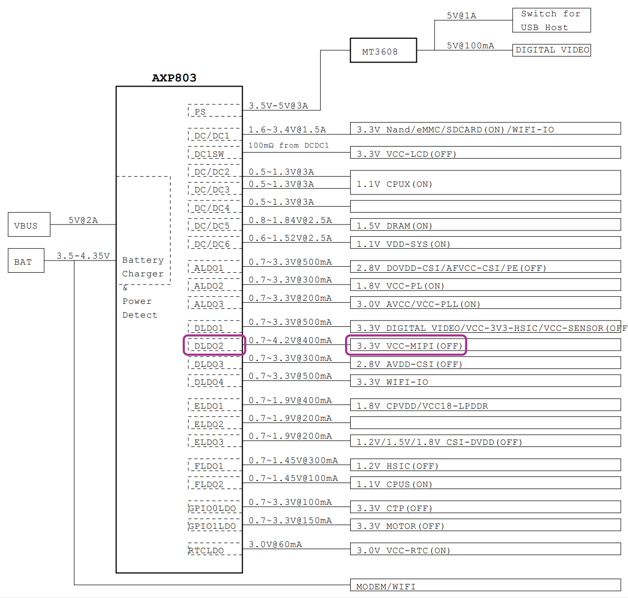
AXP803 PMIC on PinePhone Schematic (Page 3)
Earlier we talked about the sequence of steps that our Display Driver needs to follow…
This section explains how we initialise PinePhone’s Power Management Integrated Circuit (PMIC), before accessing PinePhone’s LCD Display.
To power on the LCD Display, we need to program PinePhone’s Power Management Integrated Circuit (PMIC)…
The AXP803 PMIC (pic above) is connected on Allwinner A64’s Reduced Serial Bus (RSB) (works like I2C) at RSB Address 0x2D: pmic.zig
/// Address of AXP803 PMIC on Reduced Serial Bus
const AXP803_RT_ADDR = 0x2d;
A64’s Reduced Serial Bus is explained here…
We captured the log from p-boot display_board_init…
By decoding the captured addresses and values, we decipher the following steps to initialise PinePhone’s Power Management Integrated Circuit (PMIC)…
Configure PD23 for Output
Register PD_CFG2_REG (PD Configure Register 2)
0x74 (A64 Page 387)assert reset: GPD(23), 0 // PD23 - LCD-RST (active low)
sunxi_gpio_set_cfgpin: pin=0x77, val=1
sunxi_gpio_set_cfgbank: bank_offset=119, val=1
clrsetbits 0x1c20874, 0xf0000000, 0x10000000Set PD23 to Low
Register PD_DATA_REG (PD Data Register)
0x7C (A64 Page 388)sunxi_gpio_output: pin=0x77, val=0
before: 0x1c2087c = 0x1c0000
after: 0x1c2087c = 0x1c0000 (DMB)Set DLDO1 Voltage to 3.3V
(DLDO1 powers the Front Camera / USB HSIC / I2C Sensors)
Register 0x15: DLDO1 Voltage Control (AXP803 Page 52)
dldo1 3.3V
pmic_write: reg=0x15, val=0x1a
rsb_write: rt_addr=0x2d, reg_addr=0x15, value=0x1a
Power on DLDO1
Register 0x12: Output Power On-Off Control 2 (AXP803 Page 51)
pmic_clrsetbits: reg=0x12, clr_mask=0x0, set_mask=0x8
rsb_read: rt_addr=0x2d, reg_addr=0x12
rsb_write: rt_addr=0x2d, reg_addr=0x12, value=0xd9
Set LDO Voltage to 3.3V
(GPIO0LDO powers the Capacitive Touch Panel)
Register 0x91: GPIO0LDO and GPIO0 High Level Voltage Setting (AXP803 Page 77)
ldo_io0 3.3V
pmic_write: reg=0x91, val=0x1a
rsb_write: rt_addr=0x2d, reg_addr=0x91, value=0x1a
Enable LDO Mode on GPIO0
Register 0x90: GPIO0 (GPADC) Control (AXP803 Page 76)
pmic_write: reg=0x90, val=0x3
rsb_write: rt_addr=0x2d, reg_addr=0x90, value=0x3
Set DLDO2 Voltage to 1.8V
(DLDO2 powers the MIPI DSI Connector)
Register 0x16: DLDO2 Voltage Control (AXP803 Page 52)
dldo2 1.8V
pmic_write: reg=0x16, val=0xb
rsb_write: rt_addr=0x2d, reg_addr=0x16, value=0xb
Power on DLDO2
Register 0x12: Output Power On-Off Control 2 (AXP803 Page 51)
pmic_clrsetbits: reg=0x12, clr_mask=0x0, set_mask=0x10
rsb_read: rt_addr=0x2d, reg_addr=0x12
rsb_write: rt_addr=0x2d, reg_addr=0x12, value=0xd9
Wait for power supply and power-on init
(15,000 microseconds)
wait for power supplies and power-on init
udelay 15000
Based on the above steps, we have implemented in Zig the PinePhone Driver for Power Management Integrated Circuit (PMIC)…
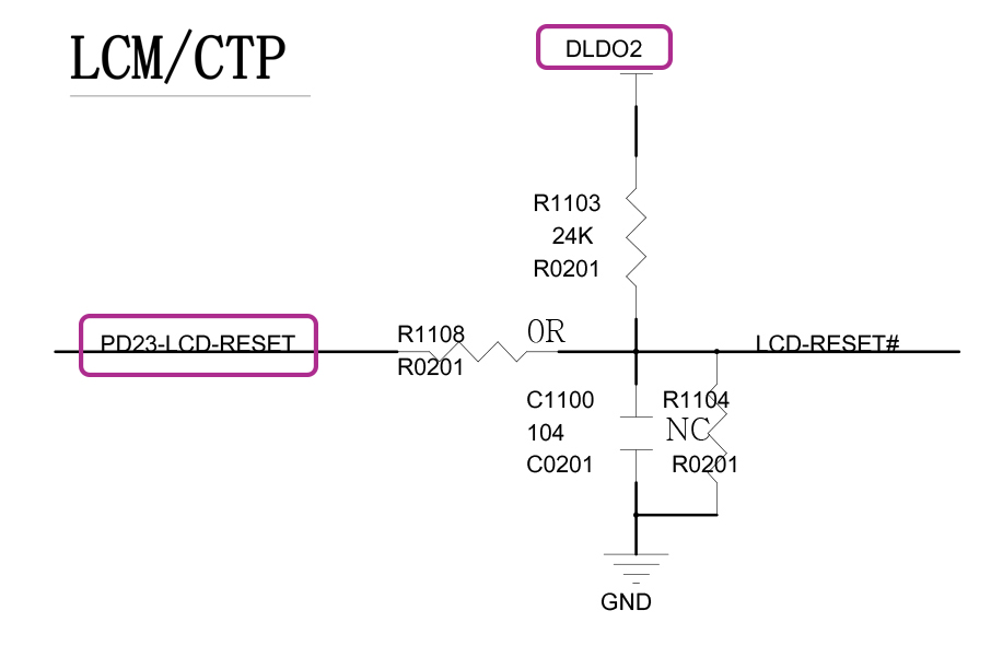
LCD Panel Reset (PD23) on PinePhone Schematic (Page 11)
Earlier we talked about the sequence of steps that our Display Driver needs to follow…
This section explains how we reset PinePhone’s LCD Panel, before sending Initialisation Commands to the ST7703 LCD Controller.
Allwinner A64 is connected to LCD Panel Reset on PD23 (LCD-RESET, pic above).
To reset the LCD Panel, we toggle PD23 Low and High like so…
Set PD23 to Low before initialising the Power Management Integrated Circuit (PMIC)
Set PD23 to High (and wait 15 milliseconds) before initialising the ST7703 LCD Controller
The complete flow for our PinePhone Display Driver looks like this: pinephone_display.c
// Turn on Display Backlight
pinephone_lcd_backlight_enable(90);

// Init Timing Controller TCON0
a64_tcon0_init(PANEL_WIDTH, PANEL_HEIGHT);

// Reset LCD Panel to Low (PD23)
pinephone_lcd_panel_reset(false);

// Init PMIC
pinephone_pmic_init();

// Wait 15 milliseconds for power supply and power-on init
up_mdelay(15);

// Enable MIPI DSI Block
a64_mipi_dsi_enable();

// Enable MIPI Display Physical Layer (DPHY)
a64_mipi_dphy_enable();

// Reset LCD Panel to High (PD23)
pinephone_lcd_panel_reset(true);

// Wait 15 milliseconds for LCD Panel
up_mdelay(15);

// Initialise LCD Controller (ST7703)
pinephone_lcd_panel_init();

// Omitted: Start MIPI DSI, init Display Engine and enable Display Engine
We captured the log from p-boot dsi_init…
By decoding the captured addresses and values, we decipher the following steps to reset PinePhone’s LCD Panel…
Configure PD23 for Output
Register PD_CFG2_REG (PD Configure Register 2)
0x74 (A64 Page 387)deassert reset: GPD(23), 1 // PD23 - LCD-RST (active low)
sunxi_gpio_set_cfgpin: pin=0x77, val=1
sunxi_gpio_set_cfgbank: bank_offset=119, val=1
clrsetbits 0x1c20874, 0xf0000000, 0x10000000Set PD23 to High or Low
Register PD_DATA_REG (PD Data Register)
0x7C (A64 Page 388)sunxi_gpio_output: pin=0x77, val=1
before: 0x1c2087c = 0x1c0000
after: 0x1c2087c = 0x9c0000 (DMB)Wait for initialization
(15 milliseconds)
wait for initialization
udelay 15000
Based on the above steps, we have implemented in Zig the PinePhone Driver that resets the LCD Panel…
We’re now porting the above driver from Zig to C. Work-in-progress…
PinePhone’s AXP803 Power Management Integrated Circuit (PMIC) is connected to Allwinner A64 via the Reduced Serial Bus (RSB)…
A64’s Reduced Serial Bus is documented in the Allwinner A80 User Manual…
“The RSB (reduced serial bus) Host Controller is designed to communicate with RSB Device using two push-pull wires.”
“It supports a simplified two wire protocol (RSB) on a push-pull bus. The transfer speed can be up to 20MHz and the performance will be improved much.”
Reduced Serial Bus seems to work like I2C, specifically for PMIC.
We’re now converting the Reduced Serial Bus Driver from Zig to C. Work-in-progress…
Base Address of Reduced Serial Bus (R_RSB) is 0x01F 03400 (A64 Page 75)
(R_RSB is implemented in the Allwinner A100 Coprocessor)
The Reduced Serial Bus Registers are (A80 Page 922)…
RSB Control Register (RSB_CTRL)
(RSB Offset 0x0000)
RSB Clock Control Register (RSB_CCR)
(RSB Offset 0x0004)
RSB Interrupt Enable Register (RSB_INTE)
(RSB Offset 0x0008)
RSB Status Register (RSB_STAT)
(RSB Offset 0x000c)
RSB Address Register (RSB_AR)
(RSB Offset 0x0010)
RSB Data Buffer Register (RSB_DATA)
(RSB Offset 0x001c)
RSB Line Control register (RSB_LCR)
(RSB Offset 0x0024)
RSB Device Mode Control Register (RSB_DMCR)
(RSB Offset 0x0028)
RSB Command Register (RSB_CMD)
(RSB Offset 0x002C)
RSB Device Address Register (RSB_DAR)
(RSB Offset 0x0030)
Here’s our implementation in Zig: pmic.zig
/// Reduced Serial Bus Offsets (A80 Page 922)
const RSB_CTRL   = 0x00;  // RSB Control Register
const RSB_STAT   = 0x0c;  // RSB Status Register
const RSB_AR     = 0x10;  // RSB Address Register
const RSB_DATA   = 0x1c;  // RSB Data Buffer Register
const RSB_CMD    = 0x2c;  // RSB Command Register
const RSB_DAR    = 0x30;  // RSB Device Address Register
The bus supports this Reduced Serial Bus Command Set (A80 Page 918)…
Set Run-Time-Address (SRTA)
(RBS Command 0xE8)
Read one byte from Device (RD8)
(RBS Command 0x8B)
Read two bytes from Device (RD16)
(RBS Command 0x9C)
Read four bytes from Device (RD32)
(RBS Command 0xA6)
Write one byte to Device (WR8)
(RBS Command 0x4E)
Write two bytes to Device (WR16)
(RBS Command 0x59)
Write four bytes to Device (WR32)
(RBS Command 0x63)
Here’s our implementation in Zig: pmic.zig
/// Read a byte from Reduced Serial Bus (A80 Page 918)
const RSBCMD_RD8 = 0x8B;

/// Write a byte to Reduced Serial Bus (A80 Page 918)
const RSBCMD_WR8 = 0x4E;
Let’s walk through the steps to…
Read a byte from RSB
Write a byte to RSB
Wait for RSB Status
Wait for RSB Transaction
To read a byte from Reduced Serial Bus…
RSB Command Register (RSB_CMD) (A80 Page 928)
0x002C0x8B (RD8) to read one byteputreg32(RSBCMD_RD8, R_RSB_BASE_ADDRESS + RSB_CMD);RSB Device Address Register (RSB_DAR) (A80 Page 928)
0x00300x2D for AXP803 PMIC)const rt_addr_shift: u32 = @intCast(u32, rt_addr) << 16;
putreg32(rt_addr_shift, R_RSB_BASE_ADDRESS + RSB_DAR);RSB Address Register (RSB_AR) (A80 Page 926)
0x0010putreg32(reg_addr, R_RSB_BASE_ADDRESS + RSB_AR);RSB Control Register (RSB_CTRL) (A80 Page 923)
0x0000putreg32(0x80, R_RSB_BASE_ADDRESS + RSB_CTRL);Wait for RSB Status
const ret = rsb_wait_stat("Read RSB");
if (ret != 0) { return ret; }
RSB Data Buffer Register (RSB_DATA) (A80 Page 926)
0x001creturn getreg8(R_RSB_BASE_ADDRESS + RSB_DATA);Here’s our implementation in Zig: pmic.zig
/// Read a byte from Reduced Serial Bus.
/// Returns -1 on error.
fn rsb_read(
  rt_addr: u8,
  reg_addr: u8
) i32 {
  // Read a byte
  debug("  rsb_read: rt_addr=0x{x}, reg_addr=0x{x}", .{ rt_addr, reg_addr });
  const rt_addr_shift: u32 = @intCast(u32, rt_addr) << 16;
  putreg32(RSBCMD_RD8,    R_RSB_BASE_ADDRESS + RSB_CMD);   // TODO: DMB
  putreg32(rt_addr_shift, R_RSB_BASE_ADDRESS + RSB_DAR);   // TODO: DMB
  putreg32(reg_addr,      R_RSB_BASE_ADDRESS + RSB_AR);    // TODO: DMB

  // Start transaction
  putreg32(0x80,          R_RSB_BASE_ADDRESS + RSB_CTRL);  // TODO: DMB
  const ret = rsb_wait_stat("Read RSB");
  if (ret != 0) { return ret; }
  return getreg8(R_RSB_BASE_ADDRESS + RSB_DATA);
}To write a byte to Reduced Serial Bus…
RSB Command Register (RSB_CMD) (A80 Page 928)
0x002C0x4E (WR8) to write one byteputreg32(RSBCMD_WR8, R_RSB_BASE_ADDRESS + RSB_CMD);RSB Device Address Register (RSB_DAR) (A80 Page 928)
0x00300x2D for AXP803 PMIC)const rt_addr_shift: u32 = @intCast(u32, rt_addr) << 16;
putreg32(rt_addr_shift, R_RSB_BASE_ADDRESS + RSB_DAR);RSB Address Register (RSB_AR) (A80 Page 926)
0x0010putreg32(reg_addr, R_RSB_BASE_ADDRESS + RSB_AR);RSB Data Buffer Register (RSB_DATA) (A80 Page 926)
0x001cputreg32(value, R_RSB_BASE_ADDRESS + RSB_DATA);RSB Control Register (RSB_CTRL) (A80 Page 923)
0x0000putreg32(0x80, R_RSB_BASE_ADDRESS + RSB_CTRL);Wait for RSB Status
return rsb_wait_stat("Write RSB");Here’s our implementation in Zig: pmic.zig
/// Write a byte to Reduced Serial Bus.
/// Returns -1 on error.
fn rsb_write(
  rt_addr: u8,
  reg_addr: u8,
  value: u8
) i32 {
  // Write a byte
  debug("  rsb_write: rt_addr=0x{x}, reg_addr=0x{x}, value=0x{x}", .{ rt_addr, reg_addr, value });
  const rt_addr_shift: u32 = @intCast(u32, rt_addr) << 16;
  putreg32(RSBCMD_WR8,    R_RSB_BASE_ADDRESS + RSB_CMD);   // TODO: DMB
  putreg32(rt_addr_shift, R_RSB_BASE_ADDRESS + RSB_DAR);   // TODO: DMB
  putreg32(reg_addr,      R_RSB_BASE_ADDRESS + RSB_AR);    // TODO: DMB
  putreg32(value,         R_RSB_BASE_ADDRESS + RSB_DATA);  // TODO: DMB

  // Start transaction
  putreg32(0x80,          R_RSB_BASE_ADDRESS + RSB_CTRL);  // TODO: DMB
  return rsb_wait_stat("Write RSB");
}To wait for status of Reduced Serial Bus…
RSB Control Register (RSB_CTRL) (A80 Page 923)
0x0000const ret = rsb_wait_bit(desc, RSB_CTRL, 1 << 7);
if (ret != 0) {
debug("rsb_wait_stat Timeout ({s})", .{ desc });
return ret;
}RSB Status Register (RSB_STAT) (A80 Page 924)
0x000cconst reg = getreg32(R_RSB_BASE_ADDRESS + RSB_STAT);
if (reg == 0x01) { return 0; }
return -1;Here’s our implementation in Zig: pmic.zig
/// Wait for Reduced Serial Bus and read Status.
/// Returns -1 on error.
fn rsb_wait_stat(
desc: []const u8
) i32 {
const ret = rsb_wait_bit(desc, RSB_CTRL, 1 << 7);
if (ret != 0) {
  debug("rsb_wait_stat Timeout ({s})", .{ desc });
  return ret;
}
const reg = getreg32(R_RSB_BASE_ADDRESS + RSB_STAT);
if (reg == 0x01) { return 0; }
debug("rsb_wait_stat Error ({s}): 0x{x}", .{ desc, reg });
return -1;
}To wait for completion of Reduced Serial Bus Transaction…
RSB Control Register (RSB_CTRL) (A80 Page 923)
0x0000// `offset` is RSB_CTRL
// `mask` is 1 << 7
const reg = getreg32(R_RSB_BASE_ADDRESS + offset);
if (reg & mask == 0) { break; } // Return 0Here’s our implementation in Zig: pmic.zig
/// Wait for Reduced Serial Bus Transaction to complete
/// Returns -1 on error.
/// `offset` is RSB_CTRL
/// `mask`   is 1 << 7
fn rsb_wait_bit(
  desc: []const u8,
  offset: u32,
  mask: u32
) i32 {
  // Wait for transaction to complete
  var tries: u32 = 100000;
  while (true) {
    // `offset` is RSB_CTRL
    // `mask`   is 1 << 7
    const reg = getreg32(R_RSB_BASE_ADDRESS + offset);
    if (reg & mask == 0) { break; }

    // Check for transaction timeout
    tries -= 1;
    if (tries == 0) {
      debug("rsb_wait_bit Timeout ({s})", .{ desc });
      return -1;
    }
  }
  return 0;
}
Check out the Notes on PinePhone’s Reduced Serial Bus.